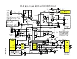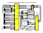
DP-4X AUDIO VIDEO MUTE CIRCUIT EXPLANATION
PAGE 02-07
(4) AC LOSS DETECTION:
AC is monitored by the AC Loss detection circuit. The AC signal generated from
PC101
photo coupler on the
Power Supply PWB to the connector
PPS1
pin (
10
). This signal is routed and rectified by
DY08
. This charges up
CY93
and through
DY08
to charge
CY92
. When AC is first applied,
CY92
charges slightly behind
CY93
pre-
venting activation of
QY47
. If AC is lost,
CY93
discharges rapidly through
RZE0
pulling the base of
QY47
low,
however
DY08
blocks
CY92
from discharging and the emitter of
QY47
is held high. This action turns on
QY47
and produces a high on its emitter. This high is routed through
DY07
and to the base of
QY57
. See the
Mute Ac-
tivation
circuit explained previously.
V MUTE 2 CIRCUITS: (
Emitter of QY42 the Mute Activation Circuit
):
The following explains the circuits affected when the Mute Activation Circuit is turned on.
CRT MUTE PATH: (
Labeled as V MUTE 1 on CRT PWB
):
The high from
QY42
is routed to
PSC
pin
11
. This high goes to
Q856
base. This transistor turns on and supplies
a ground to the following diodes,
D853
on the Green CRT PWB,
D803
on the Red CRT PWB
D8A3
on the Blue
CRT PWB. When the diodes are supplied with a low on their cathodes, they remove the base voltage for the
RGB drivers,
Q853
,
Q803
and
Q8A3
on the Green, Red and Blue CRT PWBs. This shuts off each CRT Drive.
FRONT AUDIO OUT HARD MUTE PATH:
•
The high from
QY42
(the
Mute Activation
Circuit) is routed to
DA04
. The high continues to the base of
QA10
.
When this transistor turns on, it supplies a Lo to pin
11
of
IA02
and hard mutes the Audio Out.
(Note: This is not the same thing as the Mute selected from the customer’s remote. This is controlled by
the Front Audio Control IC
IA01
internally and functions in three states, No Mute = 100%, 1/2 Mute =
50% and Full Mute = 0%.
FRONT AUDIO IC RIGHT and LEFT INPUTS MUTE PATH:
The high from
QY42
(the
Mute Activation
Circuit) is routed to
DA01
. The high continues to the bases of
QA07
and
QA08
.
When these transistors turn on the ground the Audio Front Right and Left signal input to the Audio
Output IC
IA02
and pins
4
and
2
.
MONITOR and OUT TO HI-FI MUTE PATH:
The high from
QY42
(the
Mute Activation
Circuit) is also routed to the anode of
D407
and then to the cathodes
of
D405
and
D406
. This high then arrives at the bases of
Q409,
and
Q411
.
When these transistor turns on they
ground the Right and Left audio for the Monitor Out and Out to Hi-Fi audio output jacks
J402
.
FRONT AUDIO OUT MUTE:
Labeled as V MUTE 1 (From Microprocessor Pin 49)
V MUTE 1:
The high from the Microprocessor pin
49
to
I010
(in pin
3
at 3.3V and out pin
17
at 5V). This
High is sent to the following 4 circuits:
1. To the Front Audio Out Hard Mute circuit routed through
DA06
. (
Described above
)
2. The high is also routed through
DA03
to the base of
QA01,
and
QA02
.
When these transistor turns on,
they ground the audio going into the Audio Output IC
IAA1
at the
PPS4
connector. Right audio in pin
2
of the
PPS4
connector to pin
4
of
IAA1
. Left audio in pin
3
of the
PPS4
connector to pin
2
of
IAA1
.
3.
CRT Mute:
See CRT Mute Path explanation above.
4.
Out to Hi-Fi Mute Path:
The high from the Level shifter
I007
pin
13
is routed to the anode of
DA53
and then to the cathodes of
DA51
and
DA52
to the base of
QA51,
and
QA54
.
When these transistor
turns on, they ground the audio going into the audio for Out to Hi-Fi audio output jacks.
(Continued on page 8)
Summary of Contents for 51F510
Page 2: ...DP 4X BLANK PAGE NOTES BLANK PAGE ...
Page 5: ...DP 4X CHASSIS INFORMATION POWER SUPPLY INFORMATION SECTION 1 ...
Page 6: ...DP 4X BLANK PAGE NOTES BLANK PAGE ...
Page 30: ...DP 4X BLANK PAGE NOTES BLANK PAGE ...
Page 31: ...DP 4X CHASSIS INFORMATION MICROPROCESSOR INFORMATION SECTION 2 ...
Page 32: ...DP 4X BLANK PAGE NOTES BLANK PAGE ...
Page 44: ...DP 4X BLANK PAGE NOTES BLANK PAGE ...
Page 45: ...DP 4X CHASSIS INFORMATION VIDEO INFORMATION SECTION 3 ...
Page 46: ...DP 4X BLANK PAGE NOTES BLANK PAGE ...
Page 61: ...DP 4X CHASSIS INFORMATION AUDIO INFORMATION SECTION 4 ...
Page 62: ...DP 4X BLANK PAGE NOTES BLANK PAGE ...
Page 66: ...DP 4X BLANK PAGE NOTES BLANK PAGE ...
Page 67: ...DP 4X CHASSIS INFORMATION DEFLECTION INFORMATION SECTION 5 ...
Page 68: ...DP 4X BLANK PAGE NOTES BLANK PAGE ...
Page 79: ...DP 4X CHASSIS INFORMATION DIGITAL CONVERGENCE INFORMATION SECTION 6 ...
Page 80: ...DP 4X BLANK PAGE NOTES BLANK PAGE ...
Page 94: ...DP 4X BLANK PAGE NOTES BLANK PAGE ...
Page 95: ...DP 4X CHASSIS INFORMATION CHASSIS PICTURES SECTION 07 ...
Page 96: ...DP 4X BLANK PAGE NOTES BLANK PAGE ...
Page 104: ...DP 4X BLANK PAGE NOTES BLANK PAGE ...
Page 105: ...DP 4X CHASSIS INFORMATION DP 4X CHASSIS ADJUSTMENTS SECTION 08 ...
Page 106: ...DP 4X BLANK PAGE NOTES BLANK PAGE ...
Page 108: ...DP 4X BLANK PAGE NOTES BLANK PAGE ...
Page 144: ...DP 4X BLANK PAGE NOTES BLANK PAGE ...
Page 146: ...DP 4X BLANK PAGE NOTES BLANK PAGE ...
Page 147: ...DP 4X CHASSIS INFORMATION SERVICE POLICY FOR THE DP 4X CHASSIS SECTION 10 ...
Page 148: ...DP 4X BLANK PAGE NOTES BLANK PAGE ...
Page 151: ...DP 4X BLANK PAGE NOTES BLANK PAGE ...
Page 152: ...DP 4X BLANK PAGE NOTES BLANK PAGE ...


