
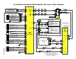


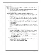


DP-4X ABL CIRCUIT EXPLANATION
PAGE 03-10
(See ABL Circuit Diagram on the next page for details)
The ABL voltage is generated from the Flyback transformer
TH01
ABL pin (
8
). The ABL pull-up resistors are
RH27
and
RH28
. They receive their pull up voltage from the
SW +115V
which is the B+ line for Deflection cre-
ated in the Power Supply.
ABL VOLTAGE OPERATION
The ABL voltage is determined by the current draw through the Flyback transformer. As the picture brightness
becomes brighter or increases, the demand for replacement of the High Voltage being consumed is greater. In
this case, the Flyback will work harder and the current through the Flyback increases. This in turn will decrease
the ABL voltage. The ABL voltage is inversely proportionate to screen brightness.
Also connected to the ABL voltage line is
DH16
. This zener diode acts as a clamp for the ABL voltage. If the
ABL voltage tries to increase above 10V due to a dark scene which decreases the current demand on the flyback,
the ABL voltage will rise to the point that
DH16
dumps the excess voltage into the 10V line.
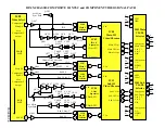
ACCL TRANSISTOR OPERATION
The ABL voltage is routed through the
PDS2
connector pin
3
to the Signal PWB. Then the ABL voltage is
routed through the acceleration circuit
RY32
and
DY01
to the base of
QY09
. Under normal conditions, this tran-
sistor is nearly saturated.
QY09
determines the voltage being supplied to the cathode of
DY02
, which is con-
nected to pin
78
of the Rainforest IC,
IY04
. During an ABL voltage decrease due to an excessive bright circum-
stance, the base of
QY09
will go down, this will drop the emitter voltage which in turn drops the cathode voltage
of
DY02
. This in turn will pull voltage away from pin
78
of the Rainforest IC,
IY04
. Internally, this reduces the
brightness, contrast and color gain voltage which is being controlled by the
I
2
C
bus data communication from the
Microprocessor arriving at pins
29
and
30
of the Rainforest IC and reduces the overall brightness, preventing
blooming as well as reducing the Color saturation level to prevent color smear.
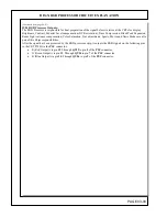
ABL SWITCH QH03
This chassis has the ability to change the Side Panels when watching a NTSC 4X3 image. When a 4X3 images is
displayed on a 16X9 set, the sides do not reach the edges. To avoid excessive ageing at the 4X3 display area, the
side panels IRE levels are raised. However, sometimes the customer may want to turn the side gray panels off.
Through the Video Advanced features Menu the customer can do this. When the Side panels are turned off, the
overall average ABL level for the image is reduced. To compensate,
QH03
ABL Switch is turned on. The Micro-
processor
I004
tells the Sub Deflection IC
IB01
via I
2
C communication
to output a high from the DAC2 line pin
2
. This high is routed through the
PPD1
connector pin
11
, to the base of
QH03
turning it
On
. This adds Resis-
tor
RH29
to the ABL pull up circuit and the ABL level drops slightly to compensate for the loss of brightness
when the side panels go black.
RH32
manipulates the trigger point of shut down dependant upon the ABL level avoiding false triggering.
NOTE: For the Circuit connected to the Xray Protect line, see the Deflection Side Shutdown Circuit Diagram for details on
Page 01-05.
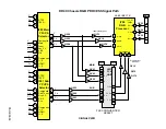
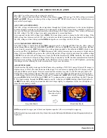
Gray Side Panels
Black Side Panels
Black Side Panels
Turned on by the
customer
Summary of Contents for 51F510
Page 2: ...DP 4X BLANK PAGE NOTES BLANK PAGE ...
Page 5: ...DP 4X CHASSIS INFORMATION POWER SUPPLY INFORMATION SECTION 1 ...
Page 6: ...DP 4X BLANK PAGE NOTES BLANK PAGE ...
Page 30: ...DP 4X BLANK PAGE NOTES BLANK PAGE ...
Page 31: ...DP 4X CHASSIS INFORMATION MICROPROCESSOR INFORMATION SECTION 2 ...
Page 32: ...DP 4X BLANK PAGE NOTES BLANK PAGE ...
Page 44: ...DP 4X BLANK PAGE NOTES BLANK PAGE ...
Page 45: ...DP 4X CHASSIS INFORMATION VIDEO INFORMATION SECTION 3 ...
Page 46: ...DP 4X BLANK PAGE NOTES BLANK PAGE ...
Page 61: ...DP 4X CHASSIS INFORMATION AUDIO INFORMATION SECTION 4 ...
Page 62: ...DP 4X BLANK PAGE NOTES BLANK PAGE ...
Page 66: ...DP 4X BLANK PAGE NOTES BLANK PAGE ...
Page 67: ...DP 4X CHASSIS INFORMATION DEFLECTION INFORMATION SECTION 5 ...
Page 68: ...DP 4X BLANK PAGE NOTES BLANK PAGE ...
Page 79: ...DP 4X CHASSIS INFORMATION DIGITAL CONVERGENCE INFORMATION SECTION 6 ...
Page 80: ...DP 4X BLANK PAGE NOTES BLANK PAGE ...
Page 94: ...DP 4X BLANK PAGE NOTES BLANK PAGE ...
Page 95: ...DP 4X CHASSIS INFORMATION CHASSIS PICTURES SECTION 07 ...
Page 96: ...DP 4X BLANK PAGE NOTES BLANK PAGE ...
Page 104: ...DP 4X BLANK PAGE NOTES BLANK PAGE ...
Page 105: ...DP 4X CHASSIS INFORMATION DP 4X CHASSIS ADJUSTMENTS SECTION 08 ...
Page 106: ...DP 4X BLANK PAGE NOTES BLANK PAGE ...
Page 108: ...DP 4X BLANK PAGE NOTES BLANK PAGE ...
Page 144: ...DP 4X BLANK PAGE NOTES BLANK PAGE ...
Page 146: ...DP 4X BLANK PAGE NOTES BLANK PAGE ...
Page 147: ...DP 4X CHASSIS INFORMATION SERVICE POLICY FOR THE DP 4X CHASSIS SECTION 10 ...
Page 148: ...DP 4X BLANK PAGE NOTES BLANK PAGE ...
Page 151: ...DP 4X BLANK PAGE NOTES BLANK PAGE ...
Page 152: ...DP 4X BLANK PAGE NOTES BLANK PAGE ...


