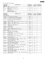


53
DP33KA/B
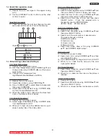
(7) Press PIP MODE key 2 times to write the changed
data in EEPROM. (First press, ADJ. PATTERN/ROM
WRITE ? 2nd press, writes data into EEPROM.
Green dots appear after completion of operation.)
(8) Press MUTE key to exit from PATTERN mode.
Adjustment Procedure
(1) Receive NTSC RF or video signal.
(2) With Power off, PRESS and HOLD the SERVICE
ONLY button on DEF./CONV. PWB, then press the
Power On/Off, when picture appears release
SERVICE ONLY button.
(Internal crosshatch is
displayed without conv. correction data.)
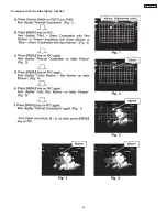
Adjustment Procedure
(1) Press FRZ key on R/C. (One addtional line appears
near the top and near the bottom.)
(2) Press VID2 key, then MAGIC FOCUS PATTERN
mode is displayed as follows:
(3) Use [6] key on remote control to rotate the arrow.
Arrow indicates each sensor position.
(Upper left
corner, middle top, upper right corner, right middle, in
this order).
(4) Use the keys to switch color of pattern.
INFO : Green pattern
0 : Red pattern
ANT : Blue pattern
(5) Press
CURSOR
F
or
E
to change the data value to
the horizontal direction. Press
CURSOR
G
or
H
to
change the data value to the vertical direction.
(6) Set the data as shown below:
RH : 0A
RV : FF
1
2
3
4
5
6
7
0
1
3
5
7
0
1
2
3
4
5
6
7
RH 00
02
fc
fe
fc
02
00
00
RV 02
00
07
00
f7
01
fd
00
GH 00
00
fc
fe
fe
00
00
00
GV 06
01
06
00
f9
00
fa
00
BH 04
fe
fe
00
00
fe
02
02
BV 08
ff
03
00
fd
01
f8
00
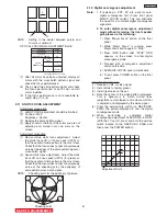
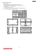
Pattern Position
Normal Mode
0
2
4
6
Pattern: 46”`
2.12.2 MAGIC FOCUS Pattern Set-Up
NOTE: (1) This instruction should be applied when a new
DCU is being replaced.
(2) This instruction shows how to set up the pattern
position for MAGIC FOCUS.
BACK TO ADJUSTMENTS
18.2 81.8 81.8 81.8 81.8 81.8 81.8 81.8 81.8 81.8 81.8 81.8 81.8 18.2
27.5
37.0
74.0
74.0
1018
573
46” (Part Number H312275)
74.0
74.0
74.0
74.0
37.0
27.5
R B
46”
Wide
2.12.3 Convergence Jig Screen Specifications
Summary of Contents for 46F500A
Page 28: ...28 DP33KA B a Adjust Mode OSD continued ...
Page 29: ...29 DP33KA B a Adjust Mode OSD continued ...
Page 30: ...30 DP33KA B a Adjust Mode OSD continued ...
Page 56: ...56 DP33KA B Convergence For Outside Signal function ...
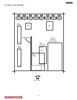
Page 111: ...PRINTED CIRCUIT BOARD SIGNAL P W B PART SIDE 111 DP33KA B TABLE OF CONTENTS ...
Page 112: ...DP33KA B PRINTED CIRCUIT BOARD SIGNAL P W B PATTERN SIDE 112 ...
Page 113: ...PRINTED CIRCUIT BOARD TERMINAL P W B PART SIDE 113 DP33KA B ...
Page 114: ...PRINTED CIRCUIT BOARD TERMINAL P W B PATTERN SIDE 114 DP33KA B ...
Page 115: ...DP33KA B PRINTED CIRCUIT BOARD POWER P W B PART SIDE 115 ...
Page 116: ...PRINTED CIRCUIT BOARD POWER P W B PATTERN SIDE 116 DP33KA B ...
Page 117: ...DP33KA B PRINTED CIRCUIT BOARD DEFLECTION P W B PART SIDE 117 ...
Page 118: ...PRINTED CIRCUIT BOARD DEFLECTION P W B PATTERN SIDE 118 DP33KA B ...
Page 119: ...DP33KA B PRINTED CIRCUIT BOARD CPT P W B PART SIDE 46F500A 119 ...
Page 120: ...PRINTED CIRCUIT BOARD CPT P W B PATTERN SIDE 120 DP33KA B ...
Page 121: ...PRINTED CIRCUIT BOARD 46F510 CONTROL P W B 121 DP33KA B ...
Page 122: ...DP33KA B PRINTED CIRCUIT BOARD DVI P W B PART SIDE 122 ...
Page 123: ...PRINTED CIRCUIT BOARD DVI P W B PATTERN SIDE 123 DP33KA B ...
Page 124: ...BLOCK DIAGRAM 124 DP33KA B TABLE OF CONTENTS ...
Page 125: ...125 DP33KA B WIRING DIAGRAM TABLE OF CONTENTS ...
Page 162: ......


