background image

50

DP33KA/B

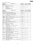
OPTICAL FOCUSING ADJUSTMENT RED

(6) In case of B lens. Set the position where the

chromatic aberration changes from purple to
green. As shown below, observe the vertical
bright line and adjust lens focus where the
purple or green chromatic aberration slightly
appears inside and purple or green outside
(reference value : 1~3mm) at the point specified
in table below.

Change the signal and fine-

adjust in the same way as the G lens.

O

I

L

NOTE:

Setting the center between Red and crimson
is optimum.

(5) In case of R lens. Set the position where the

chromatic aberration changes from red to
crimson. As shown below, observe the vertical
bright line and adjust lens focus where the
crimson or red chromatic aberration slightly
appears inside, and crimson or red outside
(reference value : 1~3mm) at the point specified
in table below.

Change the signal and fine-

adjust the same way as the G lens.

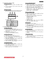
OPTICAL FOCUSING ADJUSTMENT GREEN

Change the signal to the circle pattern and fine
adjust. Observe the corner part of the screen,
especially observe number in the small circle
when adjusting. If the focus performance at the
screen center exceeds the lower limit, it is
acceptable.

CHASSIS

DP33W

SCREEN SIZE

46”

L1 and L2

(PITCHES from CENTER)

3.0

BETWEEN

L1&L2

*

COLOR

*

ABERRATION

I

2.5mm MAX

*

O

2.5mm MAX

(NOTE)

*  Slightly reddish or no color

**  Slightly bluish or no color

Small circle of circle pattern

NOTES: 1.

Since the G light is very important for
picture quality and performance, pay
special attention in its adjustment.

2.

Be careful not to touch the lens with your
fingers when adjusting.

CHASSIS

DP33W

SCREEN SIZE

46”

L1 and L2

(PITCHES from CENTER)

6.0

BETWEEN

L1&L2

*

COLOR

*

ABERRATION

I

2.0mm MAX

*

O

 2.0mm MAX

(NOTE)

*  Slightly reddish or no color

**  Slightly crimson or no color


Summary of Contents for 46F500A

Page 1: ...EMENT PARTS LIST 132 DISASSEMBLY INSTRUCTIONS 155 QUICK REFERENCE PARTS LIST IC UNIT 160 CAUTION These servicing instructions are for use by qualified service personnel only To reduce the risk of electric shock do not perform any servicing other than that contained in the operating instructions unless you are qualified to do so Before servicing this chassis it is important that the service technic...

Page 2: ...cuit boards and other components which contain lead in solder avoid unprotected skin contact with solder Also when soldering do not inhale any smoke or fumes produced This television receiver provides display of television closed captioning in accordance with section 15 119 of the FCC rules FEDERAL COMMUNICATIONS COMMISSION NOTICE This equipment has been tested and found to comply with the limits ...

Page 3: ... megohms or greater than 5 2 megohms an abnormality exists that must be corrected before the instrument is returned to the customer Repeat this test with the instrument AC switch in the off position d Leakage Current Hot Check Plug the AC line cord directly into a 120V AC 60Hz outlet do not use an isolated transformer for this check Turn the A C power ON Using a Leakage Current Tester Simpson s Mo...

Page 4: ...Do not operate the chassis longer than is necessary to locate the cause of excessive voltage h X radiation Shield 1 This receiver is provided with X ray shield plates for protection against X radiation Do not remove X ray shield plates A B or C shown in Fig 1 unnecessarily when troubleshooting and or making test measurements 2 To prevent X radiation after replacement of picture tube and lens confi...

Page 5: ...ssis can be safely serviced only with an isolation transformer inserted in the power line between the receiver and the AC power source for both personnel and test equipment protection c Some TV receiver chassis have a secondary ground system in addition to the main chassis ground This secondary ground system is not isolated from the AC power line The two ground systems are electrically separated b...

Page 6: ...is service data might be equipped 7 Do not apply AC power to this instrument and or any of its electrical assemblies unless all solid state device heat sinks are correctly installed 8 Always connect the test instrument ground lead to the appropriate instrument chassis ground before connecting the test instrument positive lead Always remove the test instrument ground lead last 9 Use with this instr...

Page 7: ...fully insert the replacement IC in the circuit board 2 Carefully bend each IC lead against the circuit foil pad and solder it 3 Clean the soldered areas with a small wire bristle brush It is not necessary to reapply acrylic coating to areas Small signal Discrete Transistor Removal Replacement 1 Remove the defective transistor by clipping its leads as close as possible to the component body 2 Bend ...

Page 8: ...e IC pin Solder the IC connection 4 Route the jumper wire along the path of the cut away copper pattern and let it overlap the previously scraped end of the good copper pattern Solder the overlapped area and clip off any excess jumper wire 1 Remove the defective copper pattern with a sharp knife Remove at least 1 4 inch of copper to ensure hazardous condition will not exist if the jumper wire open...

Page 9: ...ezers or with a miniature alligator clip and apply heat to the pad area with a 30 watt iron until solder flows Do not apply heat for more than 3 seconds How to Replace Flat lC Required Tools Soldering iron iron wire or small awl De solder braids Magnifier 1 Remove the solder from all of the pins of a Flat lC by using a de solder braid 2 Put the iron wire under the pins of the Flat lC and pull it i...

Page 10: ...d Please remove previous solder as much as possible from the soldering point When soldering please perfectly melt the lead free solder to mix well with the previous solder 3 Soldering iron for lead free solder Melting point of lead free solder is higher than solder containing lead Use of a soldering tool with temperature control and with much thermal capacitance is reccomended Reccomended temperat...

Page 11: ...perly High Voltage will be less than 31 kV at 1 72mA when TV shuts down 5 Turn off set immediately after checking circuit operation 6 Unplug set for one minute to reset shutdown circuit Remove jig and voltmeter TECHNICAL CAUTIONS TH01 AC CORD POLARITY This check is based on the UL standard Use the jigs specified by the production technology section The GND side wider blade of the AC power cord sho...

Page 12: ...annel at 10 distortion 8 ohm Impedance Max output 30 watts Anode Voltage DP33KA B 30 7 0 2kv 1 52 0 2mA Brightness 46 white screen 290cd m2 Speakers 46 2 Woofers 5 inch 12 cm round Dimensions 46F510 46F500A Height in 45 9 16 39 13 16 mm 1 157 0 1 010 5 Width in 44 7 16 44 7 16 mm 1 128 0 1 128 0 Depth in 26 7 16 24 9 16 mm 671 5 623 5 Weight lbs 161 160 kg 73 72 5 Circuit Board Assemblies C P T B ...

Page 13: ...MARK 1 Make sure the silicon cover is covering the high voltage output CAUTIONS WHEN CONNECTING DISCONNECTING THE HV CONNECTOR Perform the following when the HV connector anode connector is removed or inserted for CPT replacement etc Deflection P W B Silicon cover Wing L Position L Position Wing FBT Anode connector 3 Remove the connector slowly by pulling it away from the case During Removal 1 Rol...

Page 14: ...LUME level Press these buttons for your desired sound level The volume level will be displayed on the TV screen These buttons also serve as the cursor left F and right E buttons when in MENU mode e POWER button POWER LED Press this button to turn the TV on or off This LED light is ON during normal operation f MAGIC FOCUS Use this button to automatically adjust your picture quality to optimum perfo...

Page 15: ...ress these buttons for your desired sound level The volume level will be displayed on the TV screen These buttons also serve as the cursor left F and right E buttons when in MENU mode e POWER button Press this button to turn the TV on or off f MAGIC FOCUS Use this button to automatically adjust your picture quality to optimum performance The Magic Focus button will not work when adjustment mode is...

Page 16: ... audio cable into the left audio jack c MONITOR OUT These jacks provide fixed audio and video signals which are used for recording Use the S VIDEO Output for high quality video output d AUDIO TO HI FI Output These jacks provide variable audio output to a separate stereo amplifier With this connection the audio to the stereo can be controlled by the television s main volume e S VIDEO Inputs 3 and 4...

Page 17: ...ONTROL TABLE OF CONTENTS 0 ANT INFO VOL CH POWER TV CBL SAT DVD VCR PIP SWAP PIP MODE FREEZE DAY NIGHT MENU MUTE EXIT LAST CH REC ASPECT VIRTUAL HD SELECT SURF VID1 VID2 VID3 VID4 VID5 CLU 4324UG VIDEO CLU 4328UG DAY NIGHT ...

Page 18: ...the video program being viewed If RESET is selected only the selected input will reset to initial conditions Video Use CURSOR F or E to highlight and select Picture Mode settings Press EXIT to quit menu or select PICTURE MODE to return to previous menu Use this function to choose from automatic picture settings to optimize your TV s performance Picture Mode Contrast 100 50 Brightness 50 50 Color 5...

Page 19: ... automatically if stationary images such as digital still photos are left on the screen for more than 3 minutes 3 It may be necessary to adjust TINT to obtain optimum picture quality when using the COMPONENT VIDEO Y PBPR input jacks 4 Ant A Ant B have independent Video settings Also each of the video inputs have their own independent settings Use this function to adjust flesh tones so they appear ...

Page 20: ...ould be directly over each other to produce the white lines To simplify convergence HITACHI incorporates a function called MAGIC FOCUS located on the front control panel which allows the TV to self adjust Press this MAGIC FOCUS button and the convergence self adjustment will start and this process will take approximately 20 seconds If this button is pressed during this process no change in picture...

Page 21: ...CEL adjusted data and return to main picture Press the 1 button on the remote control to SAVE adjusted data and return to main picture Press the 2 button on the remote control to return to the manual convergence adjustment mode crosshatch pattern Press the 3 button on the remote control to recall the factory pre set convergence data NOTES 1 Please turn ON your television for at least 20 minutes be...

Page 22: ...o Prog SAP which may be a secondary language weather report etc The sources received will be displayed at the top right edge of the TV The source you select will be displayed above the sources received See example below for each selection when both stereo and second audio are received monaural is always received This function is useful when setting up the external speakers ON Select this feature i...

Page 23: ... cable 2 Way signal splitter Stereo System Amplifier L R INPUT Laserdisc player VCR camcorder etc HDTV Set Top Box DVD Player Cable TV Box OUTPUT INPUT VCR 1 ANT IN OUTPUT S VIDEO V L R ANT A TO CONVERTER ANT B L Y R MONO L AUDIO TO HI FI R S VIDEO S VIDEO S VIDEO Y VIDEO R MONO L R MONO L VIDEO R MONO L VIDEO R L VIDEO INPUT 1 INPUT 2 INPUT 3 INPUT 4 MONITOR OUT OUTPUT Y PB CB PR CR L R VCR 2 V L...

Page 24: ...pect mode to display conventional 4 3 sources by linearly increasing image expansion from the center towards the edges of the display area in order to fill it 4 3 Zoom1 Zoom2 Use these aspect modes to zoom in on conventional 4 3 sources 16 9 Standard Use this aspect mode to display 16 9 sources like HDTV and DVD s preserving the original 16 9 aspect ratio 16 9 Zoom Use this aspect mode to zoom 16 ...

Page 25: ...ster Position Adjsutment 54 2 12 5 Convergence Point Adjustment 54 2 12 6 Magic Focus Initialize 55 2 13 Blue Defocus 59 2 14 White Balance 59 2 15 Sub Brightness 60 2 16 Sub Picture Signal Amplitude Adjustment 61 2 17 Horizontal Position 62 2 18 Scanning Area Check 62 2 19 Raster Distortion Check 63 3 ADJUSTMENT POINT 64 3 1 CPT R G B Focus Pack 64 3 2 Signal Block Assembly 65 3 3 Main Chassis De...

Page 26: ...llowing pages using CURSOR G H on Remote Control Adjustable Data Others Fixed Data be careful not to change 4 Press EXIT key to exit I2C ADJUST mode NOTES 1 If the TV I2 C data is different from the I2 C Parameter of the following pages for fixed data change the data 2 When exchanging microprocessor or EEPROM and TV is turned on for first time it requires initialization of Memory Initial of I2C ad...

Page 27: ...27 DP33KA B I2 C OSD Flowchart a Adjust Mode OSD Press POWER INPUT of Control Panel ADJUSTABLE ITEM EXIT I2C ADJUST MODE EXIT OR POWER on off ...

Page 28: ...28 DP33KA B a Adjust Mode OSD continued ...

Page 29: ...29 DP33KA B a Adjust Mode OSD continued ...

Page 30: ...30 DP33KA B a Adjust Mode OSD continued ...

Page 31: ... 1 9 V FF 2 9 V Data M High Medium 7F Data S High Standard 7F Black White 00 FF 7F High 7F Medium 7F Standard 7F G CUTOFF HIGH G CUTOFF MED G CUTOFF STD G CUTOFF B W Green Cutoff Adjustment 00 1 9 V FF 2 9 V Data M High Medium 7F Data S High Standard 7F Black White 00 FF 7F High 7F Medium 7F Standard 7F B CUTOFF HIGH B CUTOFF MED B CUTOFF STD B CUTOFF B W Blue Cutoff Adjustment 00 1 9 V FF 2 9 V D...

Page 32: ... High Medium Standard Black White Standard Day Mode High Middle Low Off Middle Black Enhancement Black Enhancement Reset Adjustment High Middle Low Off Night Mode High Middle Low Off Low Day Mode High Middle Low Off High Edge Enhancement Edge Enhancement Reset Adjustment High Middle Low Off Night Mode High Middle Low Off Low DIGITAL MODULE HDTV Model only HFRQ N The number of times of Sync Frequen...

Page 33: ... 7F Data S High Standard 7F Black White 00 FF 7F G CUT H High 7F G CUT M Medium 7F G CUT S Standard 7F G CUT B Green Cutoff Adjustment 00 1 9 V FF 2 9 V Data M High Medium 7F Data S High Standard 7F Black White 00 FF 7F B CUT H High 7F B CUT M Medium 7F B CUT S Standard 7F B CUT B Blue Cutoff Adjustment 00 1 9 V FF 2 9 V Data M High Medium 7F Data S High Standard 7F Black White 00 FF 7F SUBCNT0 Su...

Page 34: ...0 232 5 degree 0F 255 degree HDTV 00 0F 03 G BGA3H High 02 G BGA3M Medium 03 G BGA3S Standard 04 G BGA3B TV NTSC Black White 05 G BGADH High 02 G BGADM Medium 03 G BGADS Standard 04 G BGADB SDTV Black White 05 G BGAEH High 00 G BGAEM Medium 00 G BGAES Standard 00 G BGAEB G Y B Y Gain 00 0 3 0F 0 45 HDTV Black White 00 0F 00 DC PNT0 DC Restoration Point 00 0 07 47 00 07 00 DCRATH High 00 DCRATM Mid...

Page 35: ...ase 00 37 5 ns 05 Normal 07 15 ns 720p 1080i ANT C PhotoMC 00 07 04 CDE 0 Color Detail Enhancer 00 min 03 max 00 03 00 DCUBRT0 RGB Brightness 00 20 IRE 7F 20 IRE 00 7F 3F DCUCNT0 RGB Contrast 00 17 dB 7F 0 dB 00 7F 5A OSDACL0 OSD Auto Contrast Limiter Switch 0 OFF 1 ON 00 01 00 OSDBRT0 OSD Brightness Adjustment 00 5 IRE 01 0 IRE 02 5 IRE 03 10 IRE 00 03 02 OSDCNT0 OSD Contrast Adjustment 00 9 5 dB...

Page 36: ...Y Gamma Switch 0 OFF 1 ON 00 01 00 YDTL 0 Y Detail Control 00 MIN Trap 0F MAX 6 dB 00 0F 07 YDELAY0 Y Group Delay Control 00 MIN Trap 0F MAX 6 dB 00 0F 09 WPPNT0 White Peak Blue Point 00 55 IRE 07 105 IRE 00 07 00 WPGA 0 White Peak Blue Gain 00 min 2 dB 07 max 9 5 dB 00 07 00 HIBRT0 High Bright Color Switch 00 OFF 01 ON 00 01 00 WPS 0 White Peak Suppressor Level 00 110 IRE 01 130 IRE 00 01 01 BLS ...

Page 37: ...MAX 00 0F 09 DCGA Chroma Motion Detection Gain 0 Gain 0 F Gain MAX 00 0F 06 VAPGA Vertical Aperture Control Gain 0 Correction OFF 7 Correction MAX x0 875 00 07 00 VAPIN Vertical Aperture Control Invert 0 Correction OFF 1F Correction MAX x0 875 00 1F 0B YHCOR Y Output High Frequency Coring 0 Coring OFF 1 Coring Small 2 Coring Center 3 Coring Large 00 03 00 TA1383F Main D9H Read Mode HSYNC M Horizon...

Page 38: ...00 03 01 Y DL2 0 Y Delay Time Adjust 2 NTSC Section 1 40 ns 2 80 ns 3 120 ns 00 03 00 AFCRAN0 Horizontal AFC Switch 0 Normal 1 Narrow 00 01 00 FDET 3 Frequency Detection Input Switch 0 480i 1 NTSC 1 480i 2 NTSC 2 D SYNC2 3 HD VD 00 03 00 HSEPL 3 ANT A B NTSC 00 HSEPL 4 480i 00 HSEPL 5 480p 00 HSEPL J Horizontal Sync Separation Level Switch 0 20 1 27 2 34 3 40 720p 1080i ANT C 00 03 00 VSEPL 3 TV N...

Page 39: ...K Detection 00 FF YGAIN Dynamic Contrast Y Gain 00 x1 7F x2 00 7F CGAIN Dynamic Contrast Color Gain 00 x1 3F x2 00 3F FC 4 Write Mode B BACK Blue Back FC Free Run Mode 0 Blue Back OFF 1 Blue Back ON 00 01 MAININ Main Input Mode 0 NTSC 1 480i 2 480p 3 720p 4 1080i 5 BM 00 0F SUBIN Sub Input Mode 0 NTSC 1 480i 2 480p 3 720p 4 1080i 00 0F VDPOS 0 VD Position Offset 00 7F 3F LINE I0 Line Interpolation...

Page 40: ...idth 5 Cyan Data Width 360 x256 90 360 x256 64 3Fh 00 3F 3F C HUECH Hue Center 5 Cyan High Bit 00 03 03 C HUECL Hue Center 5 Cyan Low Bit Data Hue 360 x1024 293 2 360 x1024 834 0342h 00 FF 42 C CLIP Sat Clip 5 Cyan 00 FF FF B SLOPE Sat Slope 6 Blue 90 00h 0 40h 90 FFh Data B SLOPE B Menu 30 1Eh 00 7F 40 B HUEW Hue Width 6 Blue Data Width 360 x256 90 360 x256 64 3Fh 00 3F 3F B HUECH Hue Center 6 Bl...

Page 41: ...INO Sub YNR Input Level Gain ANT C YPBPR DVD BM 00 07 04 MYNRRD0 Main YNR Reducing Gain 00 07 01 SYNRRD0 Sub YNR Reducing Gain 00 07 01 MYNRPS0 Main YNR Passage Level Limit 00 07 00 SYNRPS0 Sub YNR Passage Level Limit 00 07 00 MYNR0 0 Main YNR 0 Point 00 0F 07 SYNR0 0 Sub YNR 0 Point 00 0F 07 MCNRIN0 Main CNR Input Level Gain 00 07 04 SCNRIN0 Sub CNR Input Level Gain 00 07 04 MCNRRD0 Main CNR Redu...

Page 42: ...ion 0 OFF 1 ON 00 01 01 YVEDGA0 Y Vertical Edge Detection Gain 00 03 03 YVEDCR0 Y Vertical Edge coring 00 0F 04 YMDEG10 Y Motion Detection Edge Gain 1 00 07 05 YMDEC10 Y Motion Detection Edge Coring 1 00 1F 05 YMDEG00 Y Motion Detection Edge Gain 0 00 07 05 YMDEC00 Y Motion Detection Edge Coring 0 00 1F 05 YHEDGA0 Y Horizontal Edge Detection Gain 00 03 03 YHEDCR0 Y Horizontal Edge coring 00 0F 04 ...

Page 43: ...t 1080i 00 07 04 MHSHP 3 ANT A B NTSC 7F MHSHP 4 480i DVD 7F MHSHP 5 480p 7F MHSHP 6 720p 7F MHSHP 7 1080i BM 7F MHSHP Q VGA 93 MHSHP R SAM 720p 98 MHSHP S Main Horizontal Sync Horizontal Phase Offset SAM 1080i 00 FF 94 SHSHP 3 ANT A B NTSC 7F SHSHP 4 480i 7F SHSHP 5 480p 7F SHSHP 6 720p 7F SHSHP 7 Sub Horizontal Sync Horizontal Phase Offset 1080i 00 FF 7F FRMBRT0 Y Frame Bright 00 7F 60 FRMTOP0 F...

Page 44: ...e Right Position Offset for 16x9 Model Not 4 3 Standard 00 FF A6 BSLFTA0 4 3 Standard 00 BSLFTB0 Black Stretch Stop Pulse Left Position Offset for 16x9 Model Not 4 3 Standard 00 FF 59 HEGCRG0 H Edge Coring 00 1F 04 DIFCRG0 Difference Coring 00 7F 07 VE2CRG0 V Edge 2 Coring 00 1F 14 VE1CRG0 V Edge 1 Coring 00 1F 14 TCLCK 0 2 3 TV Cine Lock 00 07 03 TCUNL 0 2 3 TV Cine Unlock 00 07 00 TCARE 0 2 3 TV...

Page 45: ...ge of vertical line of the circle pattern 1 3 4 Color Management Check 1 Receive color bar signal 2 Select Color Management using CURSOR G H and then press SELECT button to display next menu 3 Select Set User Colors using CURSOR G H and then press select button to add check mark 4 Select one of the titles of color and then press SELECT button Check that selected color is changed by pressing CURSOR...

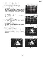
Page 46: ...ssing CURSOR E 3 Screen VR should be turned clockwise gradually and set so that retrace line begins to appear 4 Return to NORMAL mode by CURSOR F again 5 Adjust Focus VR s so that focus is even all around screen 2 2 DCU Phase Data Setting Adjustment preparation 1 Cut off adjustment should be finished 2 Set video conditions to factory preset Adjustment procedure 1 Receive any NTSC signal 2 Push SER...

Page 47: ...ter raster inclination adjustment fixing screw of DY should be screwed with 12 2kg cm torque Circle center DCU crosshatch center DCU crosshatch Circle pattern BACK TO ADJUSTMENTS 2 3 Horiontal Position Adjustment Coarse Adjustment preparation 1 DCU PHASE DATA SETTING should be finished Adjustment procedure 1 Receive circle pattern 2 Push SERVICE ONLY switch to display DCU crosshatch Mark the DCU c...

Page 48: ...cated on the DEF CONV PWB and then press the power button 6 Start adjustment 20 minutes or more after TV is turned on Adjustment procedure 1 Turn the centering magnets for red green and blue to satisfy the condition below The red and blue horizontal lines should match with green RED BLUE 46 25 35 Tolerance 2mm 1 2 Geometric center of the screen R B 2 Upon completion of adjustment fix centering mag...

Page 49: ...t line is not equal observe the side with larger chromatic aberration when adjusting 2 10 LENS FOCUS ADJUSTMENT Adjustment preparation 1 The orientation of PTV set is arbitrary west east north and south 2 Centering DY inclination should have been adjusted 3 Static focus adjustment should have been coarse adjusted 4 Drive VR location adjustment should have been completed Red 12 O clock Green 1 2 O ...

Page 50: ...nce value 1 3mm at the point specified in table below Change the signal and fine adjust the same way as the G lens OPTICAL FOCUSING ADJUSTMENT GREEN Change the signal to the circle pattern and fine adjust Observe the corner part of the screen especially observe number in the small circle when adjusting If the focus performance at the screen center exceeds the lower limit it is acceptable CHASSIS D...

Page 51: ...tment procedure 1 Red and blue static focus adjustment Adjust the static focus VR on Focus pack UFPK so that the center of circle pattern is the most clear Check that the focus does not get conspicuously worse at the edges of the circle pattern signal or cross hatch signal 2 Green static focus adjustment Adjust the static focus VR on Focus pack UFPK for green so that the center of circle pattern i...

Page 52: ...OLD the SERVICE ONLY button on DEF CONV PWB then press the Power On Off when picture appears release SERVICE ONLY switch Internal crosshatch is displayed without conv correction data 3 Press the SWAP button 2 times for ROM READ operation Picture will appear with convergence correction data Adjustment Procedure 1 Press FRZ key on R C One additional line appears near the top and near the bottom 2 Pr...

Page 53: ...op upper right corner right middle in this order 4 Use the keys to switch color of pattern INFO Green pattern 0 Red pattern ANT Blue pattern 5 Press CURSOR F or E to change the data value to the horizontal direction Press CURSOR G or H to change the data value to the vertical direction 6 Set the data as shown below RH 0A RV FF 1 2 3 4 5 6 7 0 1 3 5 7 0 1 2 3 4 5 6 7 RH 00 02 fc fe fc 02 00 00 RV 0...

Page 54: ...signal 2 Start adjustment at the center of the screen 3 Continue adjustment at next closest position 4 Adjust center area first ending with edge sections 5 Press VID3 button to perform calculation operation This process will take about 1 second and no picture will be seen at this time 6 After interpolation check convergence again and repeat 1 5 if necessary 7 When convergence is acceptable press P...

Page 55: ...o set DCU adj mode 2 Press PIP MODE key on R C Then ROM WRITE is displayed for alarm Next press PIP CH key on R C to start initialization When green dots appear initalization operation is finished NOTE If there is an error message red dots or an error code refer to page 58 CONVERGENCE ERRORS INITIAL N Initialization Operation BACK TO ADJUSTMENTS 1 2 3 4 5 6 7 8 9 0 ANT INFO VOL CH POWER TV CBL SAT...

Page 56: ...56 DP33KA B Convergence For Outside Signal function ...

Page 57: ...TMENT FLOW CHART START Cut Off Adj Blue defocus Adj Sub bright Adj Adj High Light W B Adj Low Light W B Sub bright Adj Check Low Light W B High Light W B FINISH Repeat two or three times until no adjustment is needed If NOT OK If OK ...

Page 58: ...n Outside Light 2 2 Placing of sensor 3 Is pattern hitting sensor 4 Check connection and solder bridge of sensor 5 Replace sensor 6 Replace sensor P W B 7 Sensor Connector check 8 Replace DCU 9 Adjustment check H V size centering VF Error Replace DCU 3 2 4 Over Flow 1 Check the placement of sensor 2 Adjustment check H V size centering 3 Conv amp gain check 1 check resistor values only A D Level Sa...

Page 59: ... color as a reference color then adjust Low Light W B by increasing other two colors CUT OFF data Do not change GREEN CUT OFF data CA 100 Probe should be set to a direction as shown below Repeat A B two or three times until no adjustment is needed white balance tracking GOOD If W B tracking is not good set all data Both DRV and CUT OFF to inital data and change reference color to different color N...

Page 60: ...in I2 C ADJUST mode press Input and Power button on Control panel at same time using CURSOR G H and then CURSOR E 2 Then adjust Sub Brightness using CURSOR F E to increase or decrease the value according to figure Visually adjust 3 After adjustment press MENU button to exit I2 C ADJUST mode Data is stored in memory Note When selecting SUB BRIGHTNESS mode the microprocessor sets the CONTRAST and CO...

Page 61: ...o S Video YPBPR DVI 6 Connect probe on the P852 CPT P W B Green to check sub picture amplitude Adjustment procedure 1 Go to SUB CONT TV S adj on the I2 C service mode 2 Press PIP button and MODE button of R C 3 Observe P852 on the CPT P W B and change the SUB CONT TV S I2 C data so that the amplitude of the sub picture is the same level as that of the main picture DISPLAY Main Picture Press PIP bu...

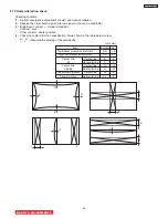
Page 62: ...set to Factory Preset Condition 3 DIGITAL CONVERGENCE adjustment should be finished Adjustment procedure NORMAL 16 9 STANDARD MODE 1 Receive circle pattern 2 Picture Format is 16 9 Standard 3 Go to I2 C Adj mode by pressing INPUT and POWER button on control panel at the same time 4 Choose H POSITION item using R C CURSOR G H 5 Adjust HORIZONTAL POSITION as follows using R C CURSOR F E Spec Balance...

Page 63: ...ition 4 Check the raster distortion specification Value shown in the table below or less A D I L Measure the winding of the outside line Item Symbol 46 Top Bottom pincushion distortion A B 5 Right Left pincushion distortion C D 4 Center line Vertical line E 5 tilt Horizontal line F 5 Center line Vertical line G 3 winding Horizontal line H 3 Trapezoidal distortion Vertical line I J 4 Skew distortio...

Page 64: ...PRT 3 CENTERING MAGNET FOR BLUE PRT 4 4 POLE MAGNET FOR BEAM FORM ADJUSTMENT 5 BEAM ALIGNMENT MAGNET 6 FOCUS PACK 1 6 4 2 3 5 4 4 5 1 CENTERING MAGNET FOR RED PRT 2 CENTERING MAGNET FOR GREEN PRT 3 CENTERING MAGNET FOR BLUE PRT 4 4 POLE MAGNET FOR BEAM FORM ADJUSTMENT 5 BEAM ALIGNMENT MAGNET 6 FOCUS PACK BACK TO ADJUSTMENTS ...

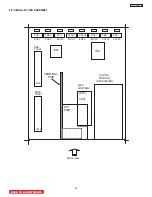
Page 65: ...SSEMBLY Sub Tuner EH7P PH2P EH13P PH10P EH2P EH10P PH12P VH12P U302 DIGITAL MODULE DP36 38 38D FLEX CONTROL PIP U401 DVI PWB TERMINAL PWB Main Tuner U301 I001 I501 Rear view PJIG PRST PFS PFSH1 PFSH2 PAS1 PBS PSC BACK TO ADJUSTMENTS ...

Page 66: ... DP33KA B 3 3 DEFLECTION P W B QH01 RH17 TH01 I601 Q777 D708 Q701 MR MG MB DF1 DIGITAL CONVERGENCE UNIT CONVERGENCE SERVICE SW IK04 IK05 XA6P PADJ SK01 V size Adj H size Adj R711 R607 BACK TO ADJUSTMENTS ...

Page 67: ...K I903 FB D932 B Green E907 B E906 B Reg E905 2 8 V E901 Audio E904 2 8 V PPC2 PA 1 2 St an d by Mo dule Main Power SW Back Cover PPQ PPV 1 3 1 3 DVD Model on ly Digital module Model on ly D955 SW 5 5V Green D913 SBY 5V Green E902 10V I902 ACK Module I903 FB D912 Main Power Red I901 T901 Switching Transformer F903 FUSE F901 FUSE PPD1 EAG1 Audio GND U901 BACK TO ADJUSTMENTS ...

Page 68: ...KA B CPT P W B RED P802 Cathode E801 GND 3 1 Screen adj VR Focus adj VR R G B B R G FOCUS PACK GREEN E851 GND 3 1 P852 Cathode FOCUS PACK UFPK P8A2 Cathode BLUE E8A1 GND 3 1 P8A1 P851 P801 BACK TO ADJUSTMENTS ...

Page 69: ...B Is base Voltage Of Q709 normal Does raster Appear with 6 and 5 Of PPD4 shorted Deflection PWB Are Voltages At both ends of T702 primary side normal Check I501 pin 37 H out I503 pin 31 DEF Hvcc etc Check T702 R748 R730 etc NO NO NO Power Supply PWB Power Supply PWB Is Power LED D913 Green ON NO YES Signal PWB Is Voltage at pin 16 of I001 3 3V Signal PWB YES Check ON I001 Check Signal PWB NO Check...

Page 70: ...k IP01 DP02 DP05 FP01 DP01 QP01 QP02 QP03 Does Red LED DP06 ìONî îBLINKî or ìOFFî DP33 W 3 No Picture Only DVD Mode No Picture Is Voltage at and of CUE8 5V Power Supply PWB Check U901 D902 PAS1 NO Signal DVD PWB Check Q031 Q032 QU94 SU91 NO YES Is click sound of Relay SU91 heard YES Check EU91 IU94 IU95 IU96 IU93 YES 6V Is Voltage at Pin 1 of IU91 6V IU91 DU91 DU95 FU91 DU92 QU91 QU92 QU93 0V Chec...

Page 71: ...d VERTICAL line or HORIZONTAL line Which has shifted VERTICAL line or HORIZONTAL line HORIZONTAL line CHECK CHANGE RK45 RK46 RV IK04 CY Amp CHECK CHANGE RK41 RK42 RH IK04 CY Amp VERTICAL line CHECK CHANGE RK61 RK62 GV IK05 CY Amp CHECK CHANGE RK57 RK58 GH IK04 CY Amp VERTICAL line HORIZONTAL line CHECK CHANGE RK53 RK54 BV IK05 CY Amp VERTICAL line CHECK CHANGE RK49 RK50 BH IK05 CY Amp Blue Green R...

Page 72: ...ECTION circuit NG CHECK RK41 42 45 46 57 58 61 62 49 50 53 54 CY Amp IK04 05 DCU CHECK DCU input 2 LK08 V BLK Ö 3 OK 1 KK56 LK06 RH KK54 LK04 GH KK52 LK02 BH 2 KK55 LK05 RV KK53 LK03 GV KK51 LK01 BV 3 LK08 V BLK Vpp 4 5 V 16 17 ms GND GND 16 17 ms GND 16 17 ms Vpp 2 5 V QK01 SW 7V Line TROUBLE SHOOTING FLOWCHART ...

Page 73: ...H SECTION Numbers inside circle correspond to locations shown in the circuit diagram 73 I001 P01 VHOLD1 I001 P13 XOUT I001 P21 OSD BLK I001 P22 HALFTONE I001 P23 M S SYNC DET I001 P28 SCL2 5 6 1 2 3 4 BACK TO TABLE OF CONTENTS ...

Page 74: ... B WAVEFORMS AT EACH SECTION Numbers inside circle correspond to locations shown in the circuit diagram 74 I001 P29 SCL1 I001 P30 SDA1 7 8 I001 P31 SDA2 I001 P32 OSD R 9 10 I001 P33 OSD G I001 P34 OSD B 11 12 ...

Page 75: ...MS AT EACH SECTION Numbers inside circle correspond to locations shown in the circuit diagram 75 I001 P46 CE FLASH I001 P52 DATA KEY 13 14 I001 P62 OSD HSYNC IN I001 P64 OSD VSYNC IN 15 16 I008 P01 Y1 I008 P02 Y0 17 18 ...

Page 76: ...DP33KA B WAVEFORMS AT EACH SECTION Numbers inside circle correspond to locations shown in the circuit diagram 76 I008 P03 Z1 I008 P04 Z 19 20 I008 P05 Z0 I008 P12 X0 21 22 I008 P13 X1 I010 P01 Vcc 23 24 ...

Page 77: ...AVEFORMS AT EACH SECTION Numbers inside circle correspond to locations shown in the circuit diagram 77 I501 P12 R OUT I501 P13 G OUT 25 26 I501 P14 B OUT I501 P35 VP OUT 27 28 I501 P37 H OUT I501 P39 FBP IN 29 30 ...

Page 78: ...ECTION Numbers inside circle correspond to locations shown in the circuit diagram 78 I601 P01 10X Reduced V OUT I601 P03 TRIGGER INPUT 31 32 I601 P07 RAMP GEN I701 P06 33 34 I901 P01 100X Reduced OCP I901 P03 100X Reduced D 35 36 ...

Page 79: ...EFORMS AT EACH SECTION Numbers inside circle correspond to locations shown in the circuit diagram 79 IH01 P01 IH01 P04 GEN 37 38 IK04 P18 PCG or CYH IK05 P09 PCG or CYV 39 40 IY03 P03 SYNC OUT IY03 P15 VD OUT 41 42 ...

Page 80: ...FORMS AT EACH SECTION Numbers inside circle correspond to locations shown in the circuit diagram 80 IY03 P26 CW OUT PPD3 P06 H DRIVE 43 44 PPD3 P08 H BLK PPD3 P10 V DRIVE 45 46 PPD3 P12 V BLK PPS3 P06 H DRIVE 47 48 ...

Page 81: ...VEFORMS AT EACH SECTION Numbers inside circle correspond to locations shown in the circuit diagram 81 PPS3 P08 H BLK PPS3 P10 V DRIVE 49 50 PPS3 P12 V BLK PST2 P31 SUB H 51 52 PST2 P32 SUB V PST2 P34 MAIN V 53 54 ...

Page 82: ...EACH SECTION Numbers inside circle correspond to locations shown in the circuit diagram 82 PST2 P35 MAIN H Q709 10X Reduced BASE 55 56 Q709 COLLECTOR Q709 EMITTER 57 58 Q777 10X Reduced BASE Q777 100X Reduced COLLECTOR 59 60 ...

Page 83: ...ECTION Numbers inside circle correspond to locations shown in the circuit diagram 83 Q777 EMITTER Q851 COLLECTOR 61 62 QH01 100X Reduced DRAIN QH02 COLLECTOR 63 64 T901 P11 100X Reduced CONTROL 115V TH01 P05 10X Reduced 50P 65 66 ...

Page 84: ...0 0 72 0 0 97 2 3 23 2 9 48 0 0 73 3 3 98 0 0 24 3 3 49 0 0 74 3 3 99 5 2 25 0 0 50 3 3 75 3 3 100 2 1 Symbol Pin No V DC Pin No V DC Symbol Pin No V DC 1 0 0 5 5 1 1 5 2 I003 2 0 0 6 5 1 2 0 0 3 0 0 7 0 0 I009 3 1 3 4 0 0 8 5 2 4 3 3 5 5 2 Symbol Pin No V DC Pin No V DC 1 0 0 9 5 2 Symbol Pin No V DC Pin No V DC 2 0 0 10 5 2 1 4 3 9 9 0 3 0 0 11 5 2 2 0 0 10 0 0 I004 4 0 0 12 0 1 3 0 0 11 0 0 5 0...

Page 85: ... Symbol Pin No V DC Pin No V DC Symbol Pin No V DC Pin No V DC 1 2 3 15 0 0 1 1 8 13 0 0 2 5 5 16 2 9 2 3 8 14 2 4 3 0 0 17 2 3 3 5 0 15 0 0 4 5 2 18 2 1 4 5 2 16 2 4 5 5 2 19 1 8 5 5 2 17 1 8 6 0 0 20 0 0 U302 6 0 0 18 2 3 U301 7 5 0 21 0 1 7 5 0 19 0 0 8 0 0 22 0 1 8 0 0 20 0 0 9 32 5 23 0 1 9 32 5 21 0 0 10 0 0 24 0 0 10 0 0 22 0 0 11 0 0 25 0 0 11 0 0 23 0 0 12 0 0 26 4 2 12 0 0 13 8 9 27 4 2 ...

Page 86: ... 2 3 Q007 C 0 0 Q035 C 0 0 E 0 0 E 2 9 B 0 1 B 2 9 Q008 C 3 0 Q036 C 5 0 E 0 0 E 2 3 B 5 8 B 0 7 Q009 C 0 5 Q037 C 0 0 E 5 0 E 0 0 B 5 2 B 0 8 Q010 C 0 0 Q038 C 0 0 E 5 8 E 0 0 B 4 9 B 0 1 Q011 C 9 1 Q039 C 3 5 E 5 2 E 0 0 B 3 6 B 0 1 Q012 C 0 0 Q040 C 3 4 E 4 2 E 0 0 B 5 0 B 2 9 Q013 C 9 1 Q041 C 0 0 E 5 3 E 3 5 B 3 5 B 3 5 Q014 C 0 0 Q042 C 4 9 E 4 2 E 2 9 B 4 9 B 0 7 Q015 C 9 1 Q044 C 0 0 E 4 3...

Page 87: ...1 6 0 0 17 4 5 Symbol Pin No V DC Pin No V DC 7 0 2 18 4 2 1 1 8 12 0 6 8 3 8 19 4 2 2 1 8 13 0 0 9 0 0 20 0 0 3 0 0 14 0 0 10 5 1 21 3 4 4 0 0 15 0 0 11 5 1 22 3 4 PFC2 5 1 0 16 1 6 U401 6 3 4 17 0 0 Symbol Pin No V DC Pin No V DC 7 3 3 18 1 8 1 0 0 26 0 0 8 0 2 19 0 0 2 0 0 27 0 0 9 0 0 20 1 8 3 0 0 28 0 0 10 0 0 21 5 0 4 0 0 29 0 0 11 0 2 22 5 0 5 0 0 30 0 0 6 0 0 31 0 0 7 0 0 32 0 0 8 0 0 33 0...

Page 88: ... 0 0 37 1 3 57 7 8 77 4 5 18 4 1 38 0 0 58 7 0 78 5 9 19 4 1 39 1 3 59 0 0 79 0 0 20 0 0 40 2 6 60 5 1 80 0 7 Symbol Pin No V DC Pin No V DC Symbol Pin No V DC Pin No V DC 1 0 3 9 0 5 1 4 6 16 9 1 2 0 3 10 0 5 2 4 6 17 0 0 3 0 3 11 0 5 3 4 6 18 4 8 I502 4 0 3 12 3 2 4 4 6 19 4 0 5 0 3 13 3 9 5 4 6 20 4 0 6 0 0 14 3 2 6 4 6 21 4 5 7 0 0 15 0 0 7 4 6 22 4 6 8 0 0 16 9 2 IA01 8 4 6 23 4 6 9 1 0 24 4 ...

Page 89: ...2 4 E 9 1 E 3 5 B 1 8 B 0 1 B 0 2 Q509 C 0 0 Q529 C 9 1 Q554 C 2 6 E 2 5 E 0 0 E 0 0 B 1 6 B 3 8 B 0 1 Q510 C 0 0 Q531 C 9 2 QA01 C 0 0 E 2 3 E 3 5 E 0 0 B 7 4 B 4 1 B 0 0 Q511 C 9 2 Q532 C 8 0 QA02 C 0 0 E 6 8 E 3 5 E 0 0 B 0 1 B 1 9 B 0 0 Q512 C 9 2 Q533 C 3 5 QA51 C 0 0 E 0 1 E 1 2 E 0 0 B 0 1 B 1 6 B 8 4 Q513 C 0 0 Q534 C 8 5 QA52 C 5 2 E 0 7 E 0 9 E 9 1 B 0 0 B 8 5 B 2 2 Q514 C 9 2 Q535 C 3 9...

Page 90: ... 4 8 49 0 0 18 3 7 50 4 3 18 0 0 50 4 3 19 3 7 51 4 3 19 4 8 51 8 8 20 0 5 52 4 3 20 5 0 52 8 8 21 4 3 53 4 3 21 1 1 53 5 1 22 3 3 54 4 3 22 0 9 54 0 0 23 3 9 55 3 5 23 1 1 55 4 8 24 3 4 56 4 0 24 0 0 56 0 0 25 4 0 57 0 1 25 0 0 57 4 8 26 4 0 58 4 2 26 4 7 58 8 8 27 0 3 59 4 3 27 4 8 59 5 1 28 4 5 60 4 2 28 5 0 60 0 0 29 4 0 61 4 3 29 0 0 61 4 8 30 3 5 62 4 3 30 4 3 62 0 0 31 4 1 63 4 2 31 2 9 63 ...

Page 91: ...0 0 E 6 0 E 2 9 B 0 2 B 2 4 B 0 1 QV08 C 0 0 QV24 C 0 0 QXA0 C 5 1 E 0 0 E 3 0 E 0 0 B 0 2 B 4 1 B 0 2 QV09 C 0 0 QV25 C 9 0 QXA1 C 4 9 E 0 0 E 3 4 E 0 3 B 4 2 B 4 3 QV13 C 8 9 QV26 C 8 4 E 3 6 E 3 7 B 4 2 B 3 9 QV14 C 0 0 QV29 C 9 0 E 3 6 E 3 2 B 1 7 B 2 9 QV15 C 0 0 QV30 C 8 4 E 2 3 E 2 3 B 4 4 B 8 4 QV16 C 8 9 QV31 C 2 6 E 3 8 E 9 0 B 1 9 B 2 6 QV17 C 0 0 QV32 C 9 0 E 2 6 E 1 9 B 4 6 B 2 3 QV18...

Page 92: ... 0 0 12 0 0 27 0 0 13 4 7 28 2 3 13 4 7 28 2 3 14 4 8 29 2 3 14 4 8 29 2 3 15 0 2 30 2 0 15 0 2 30 2 0 B 4 7 B 3 8 QY01 C 9 0 QY22 C 0 0 E 4 0 E 4 5 B 1 7 B 3 6 QY02 C 0 0 QY23 C 0 0 E 0 0 E 4 2 B 3 6 B 3 5 QY10 C 8 4 QY24 C 0 0 E 3 0 E 4 2 B 8 4 B 4 5 QY11 C 3 5 QY25 C 5 0 E 9 0 E 3 8 B 3 5 B 0 2 QY12 C 9 0 QY26 C 5 0 E 2 9 E 0 2 B 8 9 B 3 8 QY17 C 0 1 QY28 C 0 0 E 9 0 E 4 5 B 0 1 B 3 6 QY18 C 3 ...

Page 93: ... I905 2 0 0 6 5 0 3 0 0 3 29 1 7 2 4 4 8 0 0 Symbol Pin No V DC Pin No V DC 1 6 6 5 0 0 I906 2 0 0 6 6 6 3 29 1 7 2 3 4 8 0 0 Symbol Pin No V DC Pin No V DC 1 1 6 7 14 1 2 0 1 8 5 2 IAA1 3 0 1 9 30 4 4 0 1 10 0 1 5 1 6 11 4 6 6 10 3 12 13 8 B 13 6 Q901 C 23 3 E 13 3 B 0 9 Q902 C 0 4 E 0 0 B 1 6 Q903 C 0 0 E 1 6 B 0 0 Q904 C 1 6 E 0 0 B 115 2 Q905 C 0 5 E 115 6 B 6 0 Q906 C 0 0 E 6 2 B 0 1 QAA1 C 1...

Page 94: ...E 0 5 B 0 8 B 0 0 Q706 C 10 9 QN05 C 10 3 Symbol Pin No V DC E 1 4 E 0 0 1 10 6 B 0 4 B 0 1 2 1 0 Q709 C 11 1 QN06 C 1 1 3 1 4 E 0 0 E 0 0 I701 4 0 0 B 0 0 5 5 5 Q710 C 0 4 6 5 5 E 0 0 7 4 0 B 0 0 8 10 9 Q777 C 94 0 E 0 0 B 9 6 Symbol Pin No V DC QF01 C 483 0 1 6 2 E 10 2 2 10 8 S 0 4 3 0 8 QH01 D 255 6 4 2 5 G 1 7 5 1 7 B 0 6 6 0 1 QH02 C 1 7 7 0 0 E 0 0 IH01 8 0 0 B 0 1 9 4 7 QH04 C 70 6 10 4 7 ...

Page 95: ...K06 C 0 1 8 28 5 E 0 0 B 4 7 IK04 9 0 9 B 0 0 QL10 C 0 3 10 28 6 QK07 C 0 1 E 5 0 11 0 0 E 0 1 B 4 7 12 28 5 B 0 0 QL11 C 0 1 13 0 0 QK08 C 0 1 E 5 1 14 0 0 E 0 0 B 4 7 15 0 2 QL12 C 0 4 16 0 2 E 5 1 17 28 5 B 4 7 18 0 2 QL13 C 1 4 E 5 1 B 4 7 Symbol Pin No V DC QL14 C 0 4 1 0 0 E 5 0 2 5 2 B 4 7 3 27 4 QL15 C 0 2 4 28 5 E 5 1 5 28 6 B 4 7 6 0 1 QL16 C 0 6 7 0 1 E 5 1 8 28 5 B 4 7 IK05 9 0 1 QL17 ...

Page 96: ... C 0 0 QE01 C 9 2 QEA8 C 3 5 E 2 1 E 3 3 E 197 0 B 1 8 B 4 0 Q812 C 1 1 QE02 C 9 2 E 1 1 E 3 3 B 2 9 B 2 6 Q851 C 8 6 QE03 C 0 0 E 2 5 E 3 2 B 8 7 B 193 4 Q852 C 9 3 QE06 C 100 7 E 8 6 E 193 7 B 9 2 B 3 6 Q853 C 194 0 QE07 C 100 7 E 8 7 E 3 2 B 2 3 B 219 2 Q854 C 0 6 QE08 C 0 0 E 2 3 E 219 5 B 195 3 G 4 6 Q855 C 219 3 QE51 C 9 2 E 193 6 E 4 0 B 0 0 B 4 0 Q856 C 9 9 QE52 C 9 2 E 0 0 E 3 3 B 1 7 B 2...

Page 97: ...bol Pin No V DC B 3 1 1 0 0 QM04 C 9 0 PFI 2 5 2 E 2 4 3 0 0 B 0 1 4 1 3 QM05 C 5 2 E 0 0 Symbol Pin No V DC 1 3 3 2 3 3 3 3 3 4 3 3 5 0 0 6 1 7 PFS 7 5 2 8 0 0 9 9 1 10 0 0 11 1 8 12 1 6 13 0 0 Symbol Pin No V DC 1 9 0 2 0 0 3 0 0 4 2 4 5 2 5 PFT 6 0 0 7 0 0 8 0 0 9 0 0 10 0 0 11 4 9 DC VOLTAGES Control ...

Page 98: ...941 D942 4V D D952 32V ZD D949 10V D943 5V D ZD D952 24V ZD D938 4V D Voltage Control 115V I904 Short CCT Detector Over Voltage Detector Protect On Off Switch Q903 Q904 Power On Off Switch Q902 Power On Off AC Clock 60Hz Protector E906 500 Off On RED or GREEN LED AC Plug Switching Control I901 Fuse F901 10A Varistor X901 AC Input Rectifier D901 Line Filter L901 Rectifier D902 Fuse F903 5A Line Fil...

Page 99: ...c circuit diagram the value of the parts is subject to be altered for improvement Signal 1 of 3 PRODUCT SAFETY NOTE Components marked with a and shaded have special characteristics important to safety Before replacing any of these components read carefully the PRODUCT SAFETY NOTICE of this Service Manual Don t degrade the safety of the receiver through improper servicing BASIC CIRCUIT DIAGRAM DP33...

Page 100: ... the value of the parts is subject to be altered for improvement Signal 2 of 3 PRODUCT SAFETY NOTE Components marked with a and shaded have special characteristics important to safety Before replacing any of these components read carefully the PRODUCT SAFETY NOTICE of this Service Manual Don t degrade the safety of the receiver through improper servicing BASIC CIRCUIT DIAGRAM DP33KA B Signal 2 of ...

Page 101: ...ram the value of the parts is subject to be altered for improvement Signal 3 of 3 PRODUCT SAFETY NOTE Components marked with a and shaded have special characteristics important to safety Before replacing any of these components read carefully the PRODUCT SAFETY NOTICE of this Service Manual Don t degrade the safety of the receiver through improper servicing BASIC CIRCUIT DIAGRAM DP33KA B Signal 3 ...

Page 102: ...ue of the parts is subject to be altered for improvement Terminal 1 of 2 PRODUCT SAFETY NOTE Components marked with a and shaded have special characteristics important to safety Before replacing any of these components read carefully the PRODUCT SAFETY NOTICE of this Service Manual Don t degrade the safety of the receiver through improper servicing BASIC CIRCUIT DIAGRAM DP33KA B Terminal 1 of 2 10...

Page 103: ...e value of the parts is subject to be altered for improvement Terminal 2 of 2 PRODUCT SAFETY NOTE Components marked with a and shaded have special characteristics important to safety Before replacing any of these components read carefully the PRODUCT SAFETY NOTICE of this Service Manual Don t degrade the safety of the receiver through improper servicing BASIC CIRCUIT DIAGRAM DP33KA B Terminal 2 of...

Page 104: ...cuit diagram the value of the parts is subject to be altered for improvement Power Supply PRODUCT SAFETY NOTE Components marked with a and shaded have special characteristics important to safety Before replacing any of these components read carefully the PRODUCT SAFETY NOTICE of this Service Manual Don t degrade the safety of the receiver through improper servicing BASIC CIRCUIT DIAGRAM DP33KA B P...

Page 105: ...asic circuit diagram the value of the parts is subject to be altered for improvement Deflection PRODUCT SAFETY NOTE Components marked with a and shaded have special characteristics important to safety Before replacing any of these components read carefully the PRODUCT SAFETY NOTICE of this Service Manual Don t degrade the safety of the receiver through improper servicing BASIC CIRCUIT DIAGRAM DP33...

Page 106: ...the value of the parts is subject to be altered for improvement Convergence PRODUCT SAFETY NOTE Components marked with a and shaded have special characteristics important to safety Before replacing any of these components read carefully the PRODUCT SAFETY NOTICE of this Service Manual Don t degrade the safety of the receiver through improper servicing BASIC CIRCUIT DIAGRAM DP33KA B Convergence 106...

Page 107: ...m the value of the parts is subject to be altered for improvement Sensor PRODUCT SAFETY NOTE Components marked with a and shaded have special characteristics important to safety Before replacing any of these components read carefully the PRODUCT SAFETY NOTICE of this Service Manual Don t degrade the safety of the receiver through improper servicing BASIC CIRCUIT DIAGRAM DP33KA B Sensor 107 ...

Page 108: ...ram the value of the parts is subject to be altered for improvement CPT VM PRODUCT SAFETY NOTE Components marked with a and shaded have special characteristics important to safety Before replacing any of these components read carefully the PRODUCT SAFETY NOTICE of this Service Manual Don t degrade the safety of the receiver through improper servicing BASIC CIRCUIT DIAGRAM DP33KA B CPT VM 108 ...

Page 109: ...lue of the parts is subject to be altered for improvement Control PRODUCT SAFETY NOTE Components marked with a and shaded have special characteristics important to safety Before replacing any of these components read carefully the PRODUCT SAFETY NOTICE of this Service Manual Don t degrade the safety of the receiver through improper servicing BASIC CIRCUIT DIAGRAM DP33KA B Control 109 46F500 46F510...

Page 110: ...gram the value of the parts is subject to be altered for improvement DVI PRODUCT SAFETY NOTE Components marked with a and shaded have special characteristics important to safety Before replacing any of these components read carefully the PRODUCT SAFETY NOTICE of this Service Manual Don t degrade the safety of the receiver through improper servicing BASIC CIRCUIT DIAGRAM DP33KA B DVI 110 ...

Page 111: ...PRINTED CIRCUIT BOARD SIGNAL P W B PART SIDE 111 DP33KA B TABLE OF CONTENTS ...

Page 112: ...DP33KA B PRINTED CIRCUIT BOARD SIGNAL P W B PATTERN SIDE 112 ...

Page 113: ...PRINTED CIRCUIT BOARD TERMINAL P W B PART SIDE 113 DP33KA B ...

Page 114: ...PRINTED CIRCUIT BOARD TERMINAL P W B PATTERN SIDE 114 DP33KA B ...

Page 115: ...DP33KA B PRINTED CIRCUIT BOARD POWER P W B PART SIDE 115 ...

Page 116: ...PRINTED CIRCUIT BOARD POWER P W B PATTERN SIDE 116 DP33KA B ...

Page 117: ...DP33KA B PRINTED CIRCUIT BOARD DEFLECTION P W B PART SIDE 117 ...

Page 118: ...PRINTED CIRCUIT BOARD DEFLECTION P W B PATTERN SIDE 118 DP33KA B ...

Page 119: ...DP33KA B PRINTED CIRCUIT BOARD CPT P W B PART SIDE 46F500A 119 ...

Page 120: ...PRINTED CIRCUIT BOARD CPT P W B PATTERN SIDE 120 DP33KA B ...

Page 121: ...PRINTED CIRCUIT BOARD 46F510 CONTROL P W B 121 DP33KA B ...

Page 122: ...DP33KA B PRINTED CIRCUIT BOARD DVI P W B PART SIDE 122 ...

Page 123: ...PRINTED CIRCUIT BOARD DVI P W B PATTERN SIDE 123 DP33KA B ...

Page 124: ...BLOCK DIAGRAM 124 DP33KA B TABLE OF CONTENTS ...

Page 125: ...125 DP33KA B WIRING DIAGRAM TABLE OF CONTENTS ...

Page 126: ...in 10mm Anode lead must not be twisted during theoperation of wiring dress NOTE Refer to the figure 03 page when the HV connector anode lead is removed or inserted FBT N005 Ç8 PURSE LOCK ANODE R ANODE G ANODE B FS FOCUS PPD3 PPD6 PPD2 PPD1 PDC1 PDS1 CPT P W B G Åj PVMB PVMG G G FOCUS SCREEN G G FOCUS SCREEN SCREEN FOCUS SCREEN FOCUS B B G G PMB PMR PMG PS PSC SCREEN B to CPT R P W B POWER P W B DE...

Page 127: ... PL U404 Woofer L White Red U402 make one loop EGB2 SCREEN R PCR PMR PCG PCB L R 801 802 8A1 8A2 851 852 8A1 8A2 RG2 851 852 GB2 8A1 8A2 GB2 01 reference from SIGNAL P W B from DEFLECTION P W B DF1 from POWER P W B N007 DF1 N006 N006 RG2 PFT CONTROL P W B FI A specification 1 reference R DP37 37C 37D PFS DP37 37C 37D CONTROL SUB P W B PFI FI FT1 W851 ERG1 EGB1 PSC SC from SIGNAL P W B S1 S2 S3 fro...

Page 128: ...EN LEAD FROM CPT P W B LEAD COLOR ORANDE CONNECT FS CONNECTOR FROM FBT WRAPPING SOLDER DF CONNECTOR BLACK DF CONNECTOR RED NFP1 UL TUBE No 3 L 50mm CPT SOCKET HOLDER 231 234 1 Roll out silicon cover from FBT s contact area slowly 2 While turnin g the connector about 90 degrees following the arrow 0 position Push the conn ector slightly towards the case Fig A 3 Remove the connector slowly by pullin...

Page 129: ...View NOTE Some parts may appear different than those shown in the exploded view When ordering refer to the replacement parts list for the correct part number The circled numbers correspond to the parts list shown on page 142 TABLE OF CONTENTS ...

Page 130: ...6F500A 510 NOTE Some parts may appear different than those shown in the exploded view When ordering refer to the replacement parts list for the correct part number The circled numbers correspond to the parts list shown on page 142 ...

Page 131: ...OR 2003 W500 ABS 1 19 1 20 1 21 NA62121 CABI TOP COVER 1 22 NA62551 CABI COV FIX MTL 46W500 1 23 1 24 33010468 BARRIER BOARD 46F500 1 25 H512332 LOWER REAR BOARD 46W500 1 26 NA60742 BARR BRD FIX MTL L46 1 27 NA60741 BARR BRD FIX MTL R46 1 28 Red PRT ASS Y 1 29 Green PRT ASS Y 1 30 Blue PRT ASS Y 1 31 MF01101 BARRIER BOARD 46G500 1 32 NA57181 IR PWB FIX MTL DP2X 1 33 NA57577 LC METAL 2002 51 SIDE 2...

Page 132: ... 100000PFZF25V TAPE C065 0800326R CAP ELECTRO 100UF M 16V C014 0800326R CAP ELECTRO 100UF M 16V C066 0893232R CAP 1608CHIP 100000PFZF25V TAPE C015 0893239R CAP 1608CHIP 10000PFZF 50V TAPE C067 0800326R CAP ELECTRO 100UF M 16V C016 0893208R CAP 1608CHIP 1000PFKB 50V TAPE C068 0893232R CAP 1608CHIP 100000PFZF25V TAPE C017 0800282R CAP ELECTORO 2 2UF M SMG 50V C069 0800326R CAP ELECTRO 100UF M 16V C0...

Page 133: ... 16V C424 0893232R CAP 1608CHIP 100000PFZF25V TAPE C581 0893232R CAP 1608CHIP 100000PFZF25V TAPE C425 0893232R CAP 1608CHIP 100000PFZF25V TAPE C582 0800326R CAP ELECTRO 100UF M 16V C426 0800326R CAP ELECTRO 100UF M 16V C583 0893232R CAP 1608CHIP 100000PFZF25V TAPE C427 0893232R CAP 1608CHIP 100000PFZF25V TAPE C584 0893232R CAP 1608CHIP 100000PFZF25V TAPE C428 AA01101R CERAMIC CAPACITOR 1UF 10V F C...

Page 134: ...AJ00195F CAP CERAMIC CK45 F2EA472ZYNN CA33 AA00936R CERAMIC CAP 2125 X5R 4 7UF 10V C907 AJ00195F CAP CERAMIC CK45 F2EA472ZYNN CA51 0800294R CAP ELECTRO 10UF M SMG 50V C908 AL00017R ALUMINIUM ELECTROLYTIC CAP 22UF 200V CA52 0800294R CAP ELECTRO 10UF M SMG 50V C909 AL02762 CAP ELEC 680UF 200V MXC SERIES CA53 0284638R CAP ELECTRO 10UF SME BP 16V C910 AL02762 CAP ELEC 680UF 200V MXC SERIES CA54 080029...

Page 135: ...K B 50V CYLINDORICAL CH14 0279692R CAP POLYESTER 0 068UF 100V CK33 0890024M CAP CERAMIC 150PF K B 50V CYLINDORICAL CH15 0880038R CAP POLYESTER 0 0039UF KEB50V CK34 0890024M CAP CERAMIC 150PF K B 50V CYLINDORICAL CH16 AL02752 CAP ELEC 390UF 160V MXC SERIES CK36 0800355N CAP ELECTRO 470UF M 35V CH17 0800279R CAP ELECTORO 1 0UF M SMG 50V CK37 0800355N CAP ELECTRO 470UF M 35V CH18 0880198R CAP PLOY 0 ...

Page 136: ... 10V F CU96 0880194R CAP POLYESTER 0 1UF J 50V CV55 AA01111R CERAMIC CAPACITOR 1 0UF 6 3V CU97 0800319R CAP ELECTRO 47UF M 35V CV56 AA01101R CERAMIC CAPACITOR 1UF 10V F CU99 0299981F CAP POLYESTER 0 01UF J 630V CV57 AA01111R CERAMIC CAPACITOR 1 0UF 6 3V CUA2 0243509R CAP CERAMIC 470PF K 500V CV58 0800326R CAP ELECTRO 100UF M 16V CUA3 0880207R CAP POLYESTER 1 0UF J 50V CV59 0893232R CAP 1608CHIP 10...

Page 137: ...3V CY88 0800282R CAP ELECTORO 2 2UF M SMG 50V CY09 AA01111R CERAMIC CAPACITOR 1 0UF 6 3V CY89 0893213R CAP1608CHIP 2200PFKB 50V TAPE CY10 0893135R CAP 1608CHIP 470PFJCH 50V TAPE CY90 0893114R CAP 1608CHIP 12PFJCH 50V TAPE CY11 0893239R CAP 1608CHIP 10000PFZF 50V TAPE CY91 0800358R CAP ELECTRO 1000UF M 6 3V CY12 AA01101R CERAMIC CAPACITOR 1UF 10V F CY92 AA01101R CERAMIC CAPACITOR 1UF 10V F CY13 089...

Page 138: ...4041M DIODE 1SS254TA 1SS270TA D608 2344041M DIODE 1SS254TA 1SS270TA D938 2344041M DIODE 1SS254TA 1SS270TA D610 2334324M ZENER DIODE RD36E TAPE B3 SI 500MW 36V D939 2344041M DIODE 1SS254TA 1SS270TA D611 2334315M ZENER DIODE RD33E TAPE B4 D940 2344041M DIODE 1SS254TA 1SS270TA D701 CH02001M DIODE1SR139 400 D941 CH02001M DIODE1SR139 400 D706 2339882M ZENER DIODE HZS 12 A2 TAPE D942 CH02001M DIODE1SR13...

Page 139: ... SI 5MA 30 51V DL06 2331815M ZENER HZ7 B2 DH17 2344041M DIODE 1SS254TA 1SS270TA DL07 2331815M ZENER HZ7 B2 DH18 2344041M DIODE 1SS254TA 1SS270TA DL08 2331815M ZENER HZ7 B2 DJ01 CC10721R DIODE CHIP DA204K TPTX DL10 2344041M DIODE 1SS254TA 1SS270TA DJ02 CC10721R DIODE CHIP DA204K TPTX DL11 2344041M DIODE 1SS254TA 1SS270TA DJ03 CC10721R DIODE CHIP DA204K TPTX DL12 2344041M DIODE 1SS254TA 1SS270TA DJ0...

Page 140: ...R HZ12C3 TA SI 500MW I401 CK37191R MONO IC SI 3018LSA TL DU24 2331849M ZENER HZ12C3 TA SI 500MW I402 CK37406R MONO IC SI 3012KS DU25 2331849M ZENER HZ12C3 TA SI 500MW I403 CP04232 ANALOG MONOLITHIC IC BA033T DU26 2331849M ZENER HZ12C3 TA SI 500MW I404 CK37212R MONO IC TK11125CSCL DU27 2331849M ZENER HZ12C3 TA SI 500MW I453 CK37406R MONO IC SI 3012KS DU28 2331849M ZENER HZ12C3 TA SI 500MW I501 CK38...

Page 141: ...H LU02 BH00697R FILTER COIL 100UH L601 2125803N FILT COIL LHL08 27UH LU04 BH00697R FILTER COIL 100UH L602 2125803N FILT COIL LHL08 27UH LU05 BH00697R FILTER COIL 100UH L703 BH00228R COIL332K 1T7608A LU06 BM00481R LXCTZJYS51R5 4PT 01 L704 BZ05572 HORIZONTAL LINEARITY COIL 14UH LU07 BH00697R FILTER COIL 100UH L705 BZ05571 HORIZONTAL LINEARITY COIL 9UH LU91 BZ05633 LINE FILTER 10MH L801 BH00679R COIL...

Page 142: ...03 CA01271R TRS CHIP 2SC5343S Q8A5 2312372F TRS 2SC3942 Q404 CA01261R TRS CHIP 2SA1980S Q8A6 CF02771R TRS KTA1270 Q501 CA01271R TRS CHIP 2SC5343S Q8A7 CF01421R TRS KTC3198 GR TAPE Q502 CA01261R TRS CHIP 2SA1980S Q8A8 CF01421R TRS KTC3198 GR TAPE Q503 CA01271R TRS CHIP 2SC5343S Q8C2 2312372F TRS 2SC3942 Q504 CA01261R TRS CHIP 2SA1980S Q901 CF01421R TRS KTC3198 GR TAPE Q505 CA01271R TRS CHIP 2SC5343...

Page 143: ...CHIP 2SC5343S QU03 CF02771R TRS KTA1270 QY26 CA01271R TRS CHIP 2SC5343S QU04 CF01421R TRS KTC3198 GR TAPE QY28 CA01261R TRS CHIP 2SA1980S QU05 CF01421R TRS KTC3198 GR TAPE QY29 CA01261R TRS CHIP 2SA1980S QU06 CF01421R TRS KTC3198 GR TAPE QY30 CA01261R TRS CHIP 2SA1980S QU07 CF01421R TRS KTC3198 GR TAPE QY31 CA01271R TRS CHIP 2SC5343S QU91 CF02771R TRS KTA1270 QY32 CA01271R TRS CHIP 2SC5343S QU92 C...

Page 144: ... 1 16W 100 OHM R081 0790037R RES CHIP 1 16W 1 0K OHM R176 0790059R RES CHIP 1 16W 47K OHM R083 0790028R RES CHIP 1 16W 220 OHM R177 0790059R RES CHIP 1 16W 47K OHM R085 0790028R RES CHIP 1 16W 220 OHM R178 0790058R RES CHIP 1 16W 39K OHM R086 0790024R RES CHIP 1 16W 100 OHM R179 0790046R RES CHIP 1 16W 4 7K OHM R087 0790024R RES CHIP 1 16W 100 OHM R180 0790024R RES CHIP 1 16W 100 OHM R088 0790024R...

Page 145: ...1 16C16T1608 R326 0790024R RES CHIP 1 16W 100 OHM R3E5 0790001R CHIPRESISTORRECJUMPER 1 16C16T1608 R327 0790024R RES CHIP 1 16W 100 OHM R3E7 0790037R RES CHIP 1 16W 1 0K OHM R328 0790024R RES CHIP 1 16W 100 OHM R3F0 0790051R RES CHIP 1 16W 10K OHM R329 0790024R RES CHIP 1 16W 100 OHM R3F1 0790037R RES CHIP 1 16W 1 0K OHM R330 0790024R RES CHIP 1 16W 100 OHM R3F2 0790042R RES CHIP 1 16W 2 2K OHM R3...

Page 146: ...3K OHM TAPE R575 0790024R RES CHIP 1 16W 100 OHM R496 AQ00234R RES CHIP 1 16W 33K OHM TAPE R576 0790043R RES CHIP 1 16W 2 7K OHM R497 0790051R RES CHIP 1 16W 10K OHM R577 0790043R RES CHIP 1 16W 2 7K OHM R498 AQ00234R RES CHIP 1 16W 33K OHM TAPE R578 0790043R RES CHIP 1 16W 2 7K OHM R499 AQ00234R RES CHIP 1 16W 33K OHM TAPE R579 0790051R RES CHIP 1 16W 10K OHM R4A0 0790051R RES CHIP 1 16W 10K OHM ...

Page 147: ...90024R RES CHIP 1 16W 100 OHM R759 0700063M RES CARBON FLM 1 16W 47K JB R5K5 0790023R RES CHIP 1 16W 82 OHM R802 0100035M RES CARBON FLM 1 8W 56 JB R5K6 0790037R RES CHIP 1 16W 1 0K OHM R803 0100031M RES CARBON FLM 1 8W 39 JB R5K7 0790037R RES CHIP 1 16W 1 0K OHM R804 0100017M RES CARBON FLM 1 8W 10 JB R5K8 0790024R RES CHIP 1 16W 100 OHM R805 0100073M RES CARBON FLM 1 8W 2 2K JB R5K9 0790037R RES...

Page 148: ... CHIP 1 16W 12K OHM R909 AT03171S METAL OX 0 22OHM 1W RA62 0790064R RES CHIP 1 16W 100K OHM R910 AT03171S METAL OX 0 22OHM 1W RA63 0790037R RES CHIP 1 16W 1 0K OHM R911 AT03171S METAL OX 0 22OHM 1W RA64 0790063R RES CHIP 1 16W 82K OHM R912 0700038M RES CARBON FLM 1 16W 680 JB RA65 0790028R RES CHIP 1 16W 220 OHM R913 AT03844M 10 0OHM 1 2W RDS50 CARBON FILM RESISTOR RA66 0790037R RES CHIP 1 16W 1 0...

Page 149: ...ARBON FILM RESISTOR RJ25 AQ00165R RES CHIP 1 16W 82 OHM TAPE REC9 AT03895M 68KOHM 1 2W RDS50 CARBON FILM RESISTOR RJ26 0790015R RES CHIP 1 16W 22 OHM REE1 0100075M RES CARBON FLM 1 8W 2 7K JB RJ28 0790024R RES CHIP 1 16W 100 OHM REE2 AT03885M 12KOHM 1 2W RDS50 CARBON FILM RESISTOR RJ29 0790039R RES CHIP 1 16W 1 5K OHM REE3 AT03862M 220OHM 1 2W RDS50 CARBON FILM RESISTOR RJ30 0790001R CHIPRESISTORR...

Page 150: ...063M RES CARBON FLM 1 16W 47K JB RM30 0700041M RES CARBON FLM 1 16W 1 0K JB RK39 0700063M RES CARBON FLM 1 16W 47K JB RM31 0100041M RES CARBON FLM 1 8W 100 JB RK40 0700047M RES CARBON FLM 1 16W 3 3K JB RM35 0700041M RES CARBON FLM 1 16W 1 0K JB RK41 AT03213S METAL OX 8 2OHM 1W RM38 0700041M RES CARBON FLM 1 16W 1 0K JB RK42 AT03213S METAL OX 8 2OHM 1W RM41 0700032M RES CARBON RM41 0700041M RES CAR...

Page 151: ... CHIP 1 16W 1 0K OHM RU51 0790064R RES CHIP 1 16W 100K OHM RV21 0790069R RES CHIP 1 16W 270K OHM RU52 0790033R RES CHIP 1 16W 470 OHM RV22 0790069R RES CHIP 1 16W 270K OHM RU53 0790001R CHIPRESISTORRECJUMPER 1 16C16T1608 RV23 0790047R RES CHIP 1 16W 5 6K OHM RU54 0790001R CHIPRESISTORRECJUMPER 1 16C16T1608 RV24 0790047R RES CHIP 1 16W 5 6K OHM RU55 0790001R CHIPRESISTORRECJUMPER 1 16C16T1608 RV25 ...

Page 152: ...PER 1 16C16T1608 RW69 0790037R RES CHIP 1 16W 1 0K OHM RVC1 0790001R CHIPRESISTORRECJUMPER 1 16C16T1608 RW70 0790024R RES CHIP 1 16W 100 OHM RVC2 0790001R CHIPRESISTORRECJUMPER 1 16C16T1608 RW71 0790041R RES CHIP 1 16W 1 8K OHM RVC3 0790001R CHIPRESISTORRECJUMPER 1 16C16T1608 RW72 0790001R CHIPRESISTORRECJUMPER 1 16C16T1608 RVC4 0790001R CHIPRESISTORRECJUMPER 1 16C16T1608 RW76 AQ00164R RES CHIP 1 ...

Page 153: ...RES CHIP 1 16W 2 2K OHM RY05 0790037R RES CHIP 1 16W 1 0K OHM RY86 0790042R RES CHIP 1 16W 2 2K OHM RY06 AQ00174R RES CHIP 1 16W 180 OHM TAPE RY87 0790024R RES CHIP 1 16W 100 OHM RY07 AQ00192R RES CHIP 1 16W 820 OHM TAPE RY88 0790024R RES CHIP 1 16W 100 OHM RY08 0790044R RES CHIP 1 16W 3 3K OHM RY89 0790033R RES CHIP 1 16W 470 OHM RY09 0790061R RES CHIP 1 16W 56K OHM RY90 0790033R RES CHIP 1 16W 4...

Page 154: ... 5MM JST SU04 FE10402R PUSH SWITCH SKQNAB PCG ED00385 PLUG 6P LOCK 2 5MM JST SU05 FE10402R PUSH SWITCH SKQNAB PCR ED00385 PLUG 6P LOCK 2 5MM JST SU06 FE10402R PUSH SWITCH SKQNAB PDC1 ED 00383 PLUG 4P JST2 5ROCK SU91 FJ00142 RELAYALKS329 PDG ED01782 22P PLUG PIN PDS ED01782 22P PLUG PIN TRANSFORMERS PET ED03196 20P 2 5MM PITCH PLUG TAC L20P A3 T701 BT01232 HORIZONTAL OUTPUT TRANSFORMER PFC1 ED 0178...

Page 155: ...rners and pulling straight out The image at the right shows the left side of the TV only 3 The Front Door needs to be removed Loosen the top left and top right screws about half way Remove the other 4 screws Lift the Front Door up and remove 4 The following instructions are for models with a Light Box design This new cabinet design will enable servicers to remove the Light Box assembly with out th...

Page 156: ...emove 16 screws that hold the back cover assembly and screen assembly to the cabinet as shown The picture only shows one side of the TV 8 Disconnect the wiring to the right Deco Panel as shown Now move to the chassis area on the back of the TV Remove 15 screws that hold the lower rear board ...

Page 157: ...g the screen assembly completely out remove all of the wires with 4 connectors connecting to the Magic Focus sensor board first Get additional help if necessary 11 Remove the Magic Focus sensor board which is held in place by 4 plastic clips at the corners 12 Remove 3 screws which hold the lower left corner of the screen assembly ...

Page 158: ...ve 3 screws and a piece of metal slide outward that holds the right side of the back cover assembly 14 Lift the back cover assembly straight up from the cabinet The picture shows the cabinet and the Light Box assembly with the screen assembly and back cover assembly removed 15 Remove 2 screws that hold the Light Box to the cabinet 16 ...

Page 159: ...d the Light Box to the cabinet For easier removal one of the screws has to be removed from the front 18 Slightly slide the Light Box and chassis backwards until it is out Use additional help if necessary The Light Box is now ready for easy transport to a designated service and repair facility 19 Does not apply NOTE The only difference between the Disassembly Instructions for the 46F510 and 46F500A...

Page 160: ...Regulator Signal 17 I504 CP04234 BA09T 9 0V Regulator Signal 18 IA01 CK38621R NJW1160M TE1 Audio Processor w BBE and SRS Signal 19 U301 HC00514 F E ENGE6106DR Main Tuner Signal 20 U302 HC00464 F E ENG36626G Sub Tuner Signal 21 U401 CS00623 HC5623 ASS Y Flex Control Unit Signal 22 IV01 CK30941U CXA2069Q A V Selector Terminal 23 IV02 CK07631R TC90A45F Dig 2 Line Y C Separator Terminal 24 IV03 CK3481...

Page 161: ...91 TDA8147A Ver Output Deflection 47 I701 2362606 NJM4558D Gain Amp side Pin corr Deflection 48 IH01 CP07091 M62501P HV Contoller Deflection 49 IK01 CP06081 SI 3050N 5V Regulator Deflection 50 IK02 CP05011R PST994D T Mute Deflection 51 IK04 CZ01142 STK394 250 Conv Amp Deflection 52 IK05 CZ01142 STK394 250 Conv Amp Deflection 53 T701 BT01232 Horiz Output Transformer HOT Deflection 54 T702 BZ03061 L...

Page 162: ......

Reviews: