3 Development Board Circuit
3.6 Ethernet interface
DBUG385-1.1E
14(23)
3.6
Ethernet interface
3.6.1
Introduction
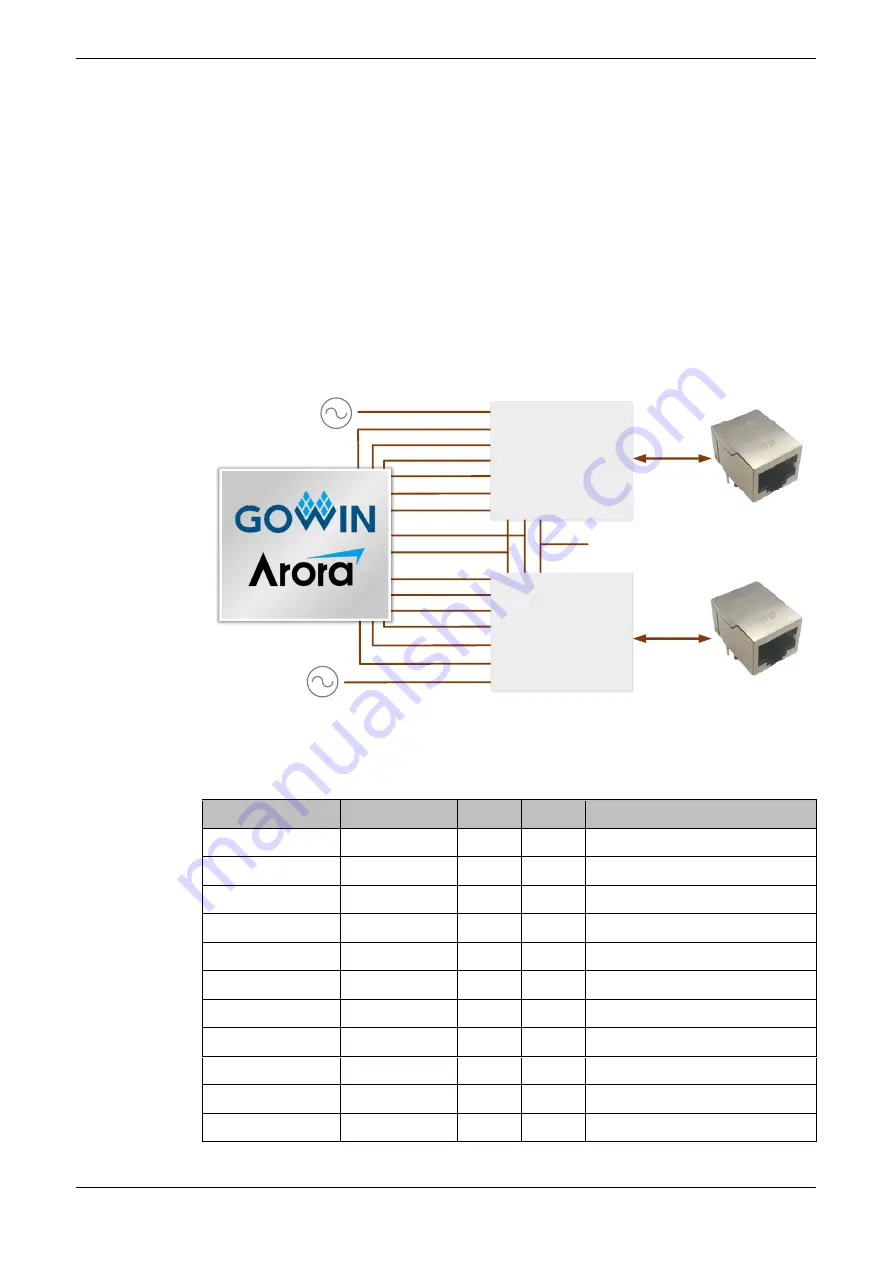
The development board has two Ethernet circuits and supports gigabit
mode, which can be used to test hardware environment in the LED display
applications, and Ethernet data transmission. The interface connected to
other devices is RJ45 with the built-in transformer. The connection diagram
is as follows:
Figure 3-5 Connection Diagram of FPGA and Ethernet
PHY1
PHY1_GTXCLK
PHY1_RXC
PHY1_TX_EN
PHY1_RX_DV
PHY1_TXD[3..0]
PHY1_RXD[3:0]
CLK_PHY1
PHY2
RST_N
PHY_MDC
PHY_MDIO
PHY2_GTXCLK
PHY2_RXC
PHY2_TX_EN
PHY2_RX_DV
PHY2_TXD[3..0]
PHY2_RXD[3:0]
CLK_PHY2
GbE 2
GbE 1
25MHz
25MHz
3.6.2
Pinout
Table 3-4 Ethernet Pinout
Signal Name
FPGA Pin No. BANK I/O
Description
PHY_MDC
M10
2
3.3V
Management channel clock
PHY_MDIO
N11
2
3.3V
Manage channel data
PHY1_GTXCLK
N10
2
3.3V
PHY1 Transmitter Clock
PHY1_TXD0
P11
2
3.3V
PHY1 sending data channel 0
PHY1_TXD1
P12
2
3.3V
PHY1 sending data channel1
PHY1_TXD2
P13
2
3.3V
PHY1 sending data channel 2
PHY1_TXD3
T11
2
3.3V
PHY1 sending data channel 3
PHY1_TX_EN
R11
2
3.3V
PHY1 sending data enable
PHY1_RXC
T12
2
3.3V
PHY1 Clock receive
PHY1_RXD0
R12
2
3.3V
PHY1 receive data channel 0
PHY1_RXD1
T13
2
3.3V
PHY1 receive data channel 1


