


User’s Manual for FD430 Digital 2-Phase Stepper Driver
User’s Manual for FD430 Digital 2-Phase Stepper Driver
7 8
3
RxD
RS232 receive
4
GND
Ground
0V
5
NC
Notice: The FD430 RS232 cable must be a special cable, which is provided according to
the user’s situation, Please confirm the cable before use to avoid damage.
4
)
LED Status Indicator
The green LED is Power indicator light, The LED turns on when the driver is powered on
and functions normally. When driver is powered off, the LED is off. The FD542 uses one
RED LED to indicate what protection has been activated. The red LED blinks
periodically (in every 3 seconds) to indicate the error type. When the fault is cleared by
the user, the red LED is always off. The specific relationship is shown in the following
table.
Number
Time(s) of
Blink
Sequence wave of Red LED
Description
1
1
Over current protection
or Single short circuit
between two phases
2
2
Over Voltage protection
3
3
No definition
4
4
No definition
2.
Control Signal Connector Interface
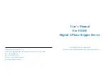
This FD430 driver uses differential inputs to increase noise immunity and interface
flexibility. Single-ended (common-cathode or common- anode) control signals from the
controller can also be accepted by this interface. The input circuit has built-in high-speed
opto-coupler, and can accept signals in the format of line driver, open-collector, or PNP
output. Recommend use line driver control signals to increase noise immunity of the
driver in interference environments.
In the following figures, connections to open-collector and PNP signals are illustrated.
Note: When VCC is 4.5V~28Vdc, R is connected or not.
3.
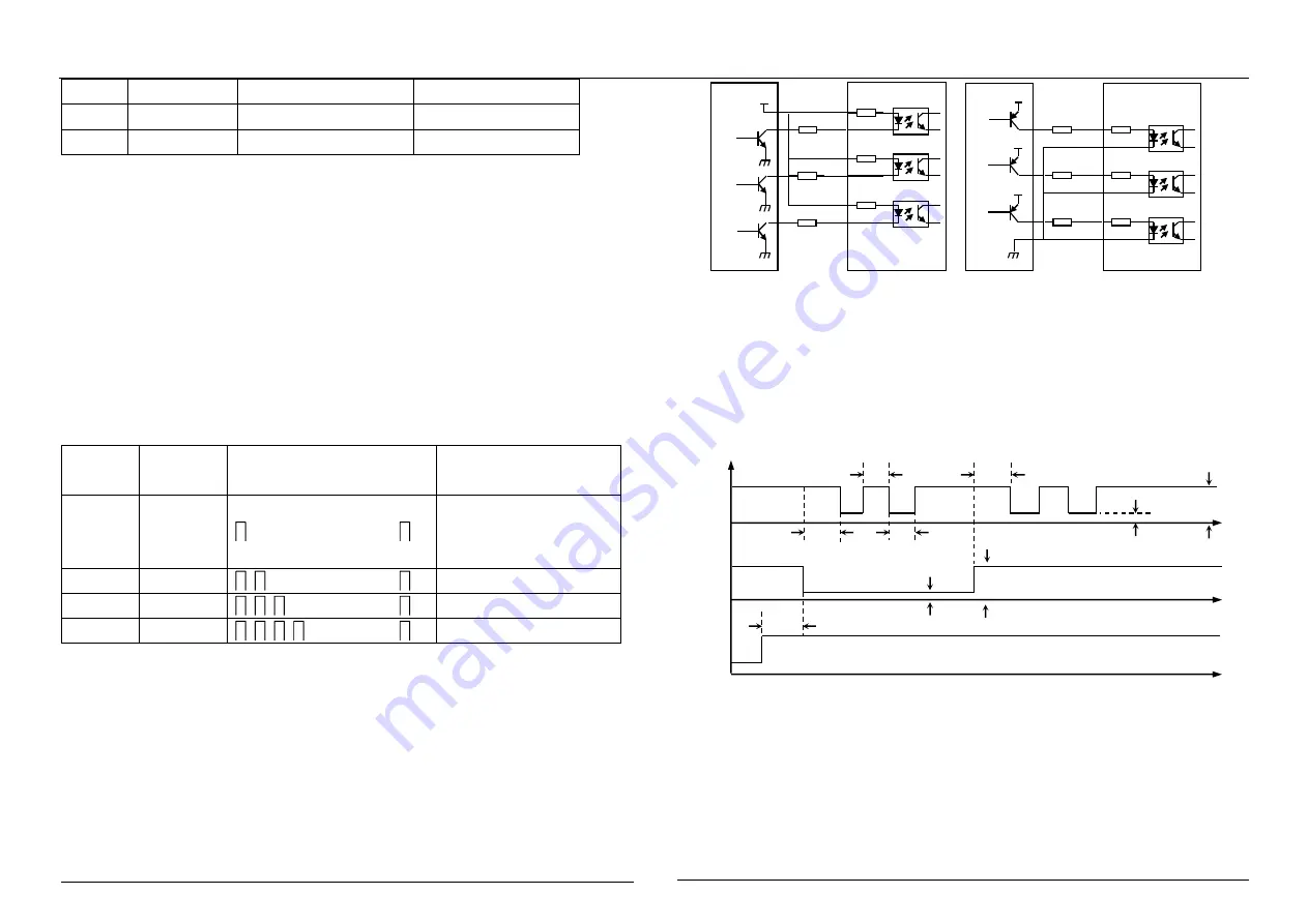
Sequence Chart of Control Signals
In order to avoid some fault operations and deviations, PUL, DIR and ENA should abide
by some rules, shown as following diagram:
Note
:
1
)
t1: ENA must be ahead of DIR by at least 5us. Determined high level. Usually,
ENA+ and ENA- are NC (not connected).
2
)
t2: DIR must be ahead of PUL active edge by 2ms to ensure correct direction;
3
)
t3: Pulse width not less than 2s;
4
)
t4: Low level width not less than 2us
.
270
Ω
270
Ω
270
Ω
Driver
PUL+
PUL-
DIR+
ENA+
DIR-
ENA-
VCC
R
R
R
脉冲信号
方向信号
使能信号
Common Anode connection
Common Cathode connection
270
Ω
270
Ω
270
Ω
Driver
PUL+
PUL-
DIR+
ENA+
DIR-
ENA-
VCC
R
R
R
脉冲信号
VCC
方向信号
VCC
使能信号
Figure 3: Input interface Circuit
t2
t4
t1
t3
t2
PUL
DIR
ENA
>2us
>2us
>5us
高电平高于
3.5V
高电平高于
3.5V
低电平低于
0.5V
低电平低于
0.5V
Figure 4 Sequence chart of control signals


