20
3. Schematics
FinePix S5100/S5500 Service Manual
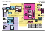
3-3. Description of Main Block Functions
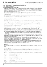
3-3-1. Technical Overview
CCD signal processing/Camera circuit section
Analog signals output from the 1/1.7 type square pixels CCD (IC701), with an effective pixel count of 4.0 mega-pixels,
undergo false color compensation processing, adaptive interpolation processing, amplification (AGC) and signal
mixing inside the CCD signal processing IC “AFE (IC103)” before being converted to 14-bit digital signals (A/D) and
sent to the signal processing LSI “UCS2 (IC201)”.
The vertical drive IC (IC101) for driving the CCD and the horizontal drive IC (IC102) are in this block.
Motor Circuit Section
The signal processing LSI “UCS2 (IC201)” that has received various operating switch commands manages the motor
drive IC (IC651) and controls the AF, SHUTTER, ZOOM and IRIS motors.
Imaging and Signal Processing Section
Input data from the CCD
14-bit digital image data (corresponding to 1H) that has been output from the imaging section (CCD/Camera Block) is
sent to the signal processing LSI “UCS2 (IC201)”, converted to 32-bit (16-bit x 2) data by the [internal buffer] inside this
LSI, and the image data for one frame (2272 x 1704 pix) is stored temporarily in [SD-RAM]. It is also integrated in the
[AUTO operation section] using the 32-bit the signal processing LSI “UCS2 (IC301)” image data and sent to the
AFE_IC (IC103) to obtain the appropriate AE/AF/AWB.
Record processing to xD Card
Image data stored in SD-DRAM “IC203” is sent one frame at a time to the internal [signal processing section] in the
signal processing LSI “UCS2 (IC201)”. In a process called unpacking, “32-bit to 12-bit conversion” and “pre-
processing including digital clamp, white balance and noise reduction processing, linear matrix processing, gamma
correction and R/G/B 14-bit to R/G/B 8-bit conversion” to “8-bit digital R/G/B signals to Y:Cb:Cr = 4:2:2 YC processing”
are implemented in this [signal processing section] and 8-bit Y/Cb/Cr image data are sent to the [internal buffer].
* Noise reduction processing, linear matrix processing and gamma correction included here are processed by the
Partner chip.
The “rearrangement of data in a format in which 8-bit Y/Cb/Cr signals are easily compressed” is done in the [internal
buffer] and after passing through the [JPEG operation block] to the [media controller], they are recorded on the xD card.
Reproduction of images from xD card
Compressed image data from the xD card is sent as 8-bit image data to the signal processing LSI “UCS2 (IC201)”
then it is sent to the [media control section], the [DMA unit] and the SD-DRAM “IC203” and then it is sent to the [media
controller], to the [JPEG operation section] and to the [signal processing section].
In the [signal processing section], 8-bit Y/Cb/Cr signals are converted to 8-bit R/G/B signals and at the same time,
lettering display signals are weighted and passed through the [LCD controller to the LCD/EVF unit and displayed.
Image capture system adjustment data are stored in the Flash ROM (IC204).
LCD/EVF Unit
Digital signals sent from the signal processing LSI “UCS2 (IC201)” are sent LCD/EVF drive IC (IC401), controls LCD/
EVF.
Power Supply Section
Power supply circuits constructed in the core of the DC IC (IC503) create the following power supplies, which are
supplied to each block.
D3.3V
[IC651 (MOTOR BLOCK), IC203 (SDRAM), IC201 (UCS2), IC204 (Flash Rom), IC202 (PARTNER), IC301
(IPS), LCD (CN401), MODE FPC]
D5.2V
[IC651 (MOTOR BLOCK)]
-7.5V
[IC701 (CCD), IC101 (V_Drv)]
15V
[IC701 (CCD), IC101 (V_Drv)]
CAM3.3V
[IC101 (V_Drv), IC102 (RTG),IC103(AFE)]
1.5V
[IC201 (UCS2), IC202 (PARTNER)]
2.5V
[IC201 (UCS2)]
MOT3.4V
[IC651 (MOTOR BLOCK), IC701 (AUDIO BLOCK)]
AD_3.3V
[IC11 (AUDIO BLOCK), IC51 (VIDEO BLOCK)]
Summary of Contents for FinePix S5100
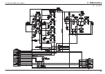
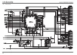
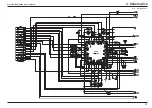
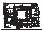
Page 23: ...23 3 Schematics FinePix S5100 S5500 Service Manual 3 6 Circuit Diagrams 3 6 1 CAM BLOCK ...
Page 24: ...24 3 Schematics FinePix S5100 S5500 Service Manual 3 6 2 DCDC BLOCK ...
Page 25: ...25 3 Schematics FinePix S5100 S5500 Service Manual 3 6 3 KSW BLOCK ...
Page 26: ...26 3 Schematics FinePix S5100 S5500 Service Manual 3 6 4 LCD EVF BLOCK ...
Page 27: ...27 3 Schematics FinePix S5100 S5500 Service Manual 3 6 5 MOTOR BLOCK ...
Page 28: ...28 3 Schematics FinePix S5100 S5500 Service Manual 3 6 6 PROCESS BLOCK ...
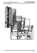
Page 29: ...29 3 Schematics FinePix S5100 S5500 Service Manual 3 6 7 CCD FPC BLOCK ...
Page 30: ...30 3 Schematics FinePix S5100 S5500 Service Manual 3 6 8 IPS STROBE BLOCK ...
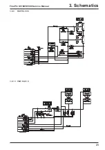
Page 31: ...31 3 Schematics FinePix S5100 S5500 Service Manual 3 6 9 MSW BLOCK 3 6 10 RSW BLOCK ...
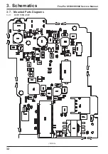
Page 33: ...33 3 Schematics FinePix S5100 S5500 Service Manual SIDE B ...
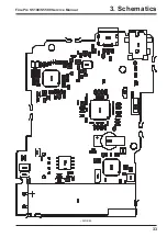
Page 34: ...34 3 Schematics FinePix S5100 S5500 Service Manual 3 7 2 MAIN PWB ASSY SIDE A ...
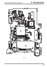
Page 35: ...35 3 Schematics FinePix S5100 S5500 Service Manual SIDE B ...
Page 36: ...36 3 Schematics FinePix S5100 S5500 Service Manual 3 7 3 KSW FPC ASSY SIDE A ...
Page 37: ...37 3 Schematics FinePix S5100 S5500 Service Manual SIDE B ...
Page 38: ...38 3 Schematics FinePix S5100 S5500 Service Manual 3 7 4 MSW FPC ASSY SIDE A ...
Page 39: ...39 3 Schematics FinePix S5100 S5500 Service Manual SIDE B ...
Page 40: ...40 3 Schematics FinePix S5100 S5500 Service Manual 3 7 5 RSW FPC ASSY SIDE A SIDE B ...
Page 41: ...41 3 Schematics FinePix S5100 S5500 Service Manual SIDE A SIDE B 3 7 6 CCD FPC ASSY ...
Page 96: ...26 30 Nishiazabu 2 chome Minato ku Tokyo 106 8620 Japan FUJI PHOTO FILM CO LTD ...

