


Notes
Func 2
Func 1
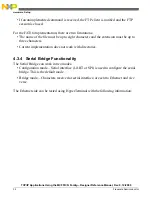
Name
Pin
PTC3 (RST)
RESET
24
Shared
PTD6 (BKGD)
BKGD
41
Analog MUX Selector
GPIO (SELECT-
OR)
PTE3
46
Demo System
Selection by Analog
MUX
ADP3 (POT)
SPSCK2 (ACC)
PTD7
42
GPIO (SD)
MISO2 (ACC)
PTE0
43
MOSI2 (ACC)
PTE1
44
GPIO (LED)
SS2 (ACC)
PTE2
45
SS1 (SD)
PTB2
15
Selection by Analog
MUX
MOSI1 (SD)
GPIO (CTS)
PTC5
30
MISO1 (SD)
SCL2 (TEMP)
PTC6
31
SPSCK1 (SD)
SDA2 (TEMP)
PTC7
32
TXD1 (RS232)
PTD0
33
RXD1 (RS232)
PTD1
34
TXD2 (RS485)
PTD2
35
RXD2 (RS485)
PTD3
36
KBI2P4 (SW2)
PTE4
47
KBI2P5 (SW1)
PTE5
48
GPIO (RTS)
PTC4
29
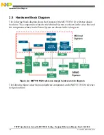
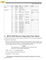
2.7 MCF51CN128 Reference Design Board Power Options
The following figure shows the power options for the MCF51CN128 reference design board.
The options are listed below:
• Ethernet—Brown and blue pairs take power. Brown pair (pin 4 and 5) is positive and
blue pair (pin 7 and 8) is negative. The voltage drop due to the Ethernet cable length
must be considered when carrying power through the RJ45 cable.
Note
This is not power over Ethernet (PoE) but a way to power-up
the MCF51CN128 reference design board.
• UART—Pin 6, +5.5 V unregulated power
• Power jack connector (Default Power Source)
• Regulated 3.3 V jack connector
TCP/IP Applications Using the MCF51CN Family—Designer Reference Manual, Rev. 0, 12/2009
19
Freescale Semiconductor
Chapter 2 Hardware Description


