


Σ
YG-S7G2-43C-MDK User’s
Manual
11/18/2015
Copyright ©2015,
Future Designs, Inc
Page
17
of
28
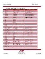
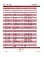
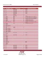
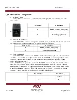
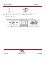
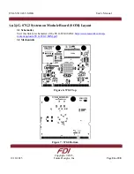
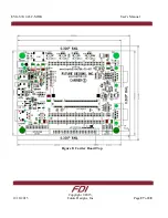
3.5
200-pin SOMDIMM Connector Details J4
Pin
SOMDIMM Signal Name
Application Details
I/O
SOMDIMM Connection Details
1
ETH_TXP
Ethernet Transmit Positive
O
Output from KSZ8041 Ethernet PHY
2
ETH_RXP
Ethernet Receive Positive
I
Output from KSZ8041 Ethernet PHY
3
ETH_TXN
Ethernet Transmit Negative
O
Input to KSZ8041 Ethernet PHY
4
ETH_RXN
Ethernet Receive Negative
I
Input to KSZ8041 Ethernet PHY
5
3V3A
3.3V Analog
P
Analog 3.3V Output from PHY Circuit
6 GND
Ground
P
7
ETH_LED0
Ethernet LED0
O
Ethernet LED0 output from KSZ8041
8
ETH_LED1
Ethernet LED1
O
Ethernet LED1 output from KSZ8041
9
VBAT_IN
Vdd Battery Input
P
Vdd for battery backup of internal RTC
10 NC
Not
Connected
U
11
RSTIN#
Reset Input
I
Reset input to POR IC TPS3801
12
RST#
O
Reset output from POR circuit
13
GPIO13_USB_ID
14 NC
Not
connected
U
15
NC
Not connected
U
16 NC
Not
connected
U
17
NC
Not connected
U
18 NC
Not
connected
U
19
NC
Not connected
U
20 NC
Not
connected
U
21
AVCC
22 AVCC
23
AVSS
24 GND
Ground
P
25
GPIO25_LCDPWR
LCD Power Enable
O
Connected to S7G2 Port 2 bit 0
26
GPIO26_LCDLE
LCD Latch Enable
O
Connected to S7G2 Port 2 bit 1
27
GPIO27_LCDCLK
LCD Clock
O
Connected to S7G2 Port 2 bit 2
28
GPIO28_LCDFP
O
Connected to S7G2 Port 2 bit 3
29
GPIO29_LCDEN
O
Connected to S7G2 Port 2 bit 4
30
GPIO30_LCDLP
O
Connected to S7G2 Port 2 bit 5
31
GPIO31_LCDVDR4
LCD Data Bit 4
O
Connected to S7G2 Port 2 bit 6
32
GPIO32_LCDVDR5
LCD Data Bit 5
O
Connected to S7G2 Port 2 bit 7
33
GPIO33_LCDVDR6
LCD Data Bit 6
O
Connected to S7G2 Port 2 bit 8
34
GPIO34_LCDVDR7
LCD Data Bit 7
O
Connected to S7G2 Port 2 bit 9
35
GPIO35_SSLB2
GPIO
U
Connected to S7G2 Port 2 bit 10
36
GPIO36
GPIO
U
Connected to S7G2 Port 2 bit 11
37
3.3V
3.3V Power
P
38 GND
Ground
P
39
3.3V
3.3V Power
P
40 GND
Ground
P
41
USBH_DP
USB Host Data Positive
B
Connected to S7G2 USB Port A D+
42
USBD_DP
USB Device Data Postive
B
Connected to S7G2 USB Port B D+
43
USBH_DM
USB Host Data Negative
B
Connected to S7G2 USB Port A D-
44
USBD_DM
USB Device Data Negative
B
Connected to S7G2 USB Port B D-
45
GPIO45_LCD_B2
46 GPIO46_LCD_B3
47
GPIO47_RD
GPIO / CAN Receive Data
I
Connected to S7G2 Port 0 bit 0
48
GPIO48_TD
GPIO / CAN Transmit Data
O
Connected to S7G2 Port 0 bit 1
49
GPIO49
GPIO
B
Connected to S7G2 Port 0 bit 2
50 NC
Not
connected
U
51
GPIO51_SPCK
52 GPIO52
53
GPIO53_MISO