Hardware Documentation efus™A9X+ efus™A9Xr2
| 14
J1
Pin Use on base board
I/O
Remarks; onboard pullups
1.12->
1.20
change
220 NC
221 USB_DEV_OC
I*
222 NC
223 USB_DEV_ID
I
100k pull up
224 GND
PWR
225 USB_DEV_N
I/Odiff
226 NC
227 USB_DEV_P
I/Odiff
228 NC
229 GND
PWR
230 GND
PWR
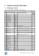
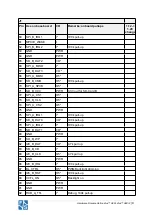
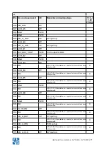
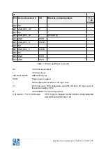
Table 1: 230 pin goldfinger connector
O5:
3.3V 5mA logic output
I:
3.3V logic input
Idiff, Odiff, I/Odiff:
differential signal
PWR:
Power input or output
*:
SW configurable as GPIO; 3.3V logic level
(*):
2.8V logic level, SW configurable as GPIO; driving 3.3V logic level on
this pin will destroy CPU!
#:
not available in all mounting options
X at column 1.12->1.20 change:
CPU IO pin is changed for this function. Only supported
with SW built for HW Rev 1.20


