background image

ALUDRA user manual 

Issue A


66 

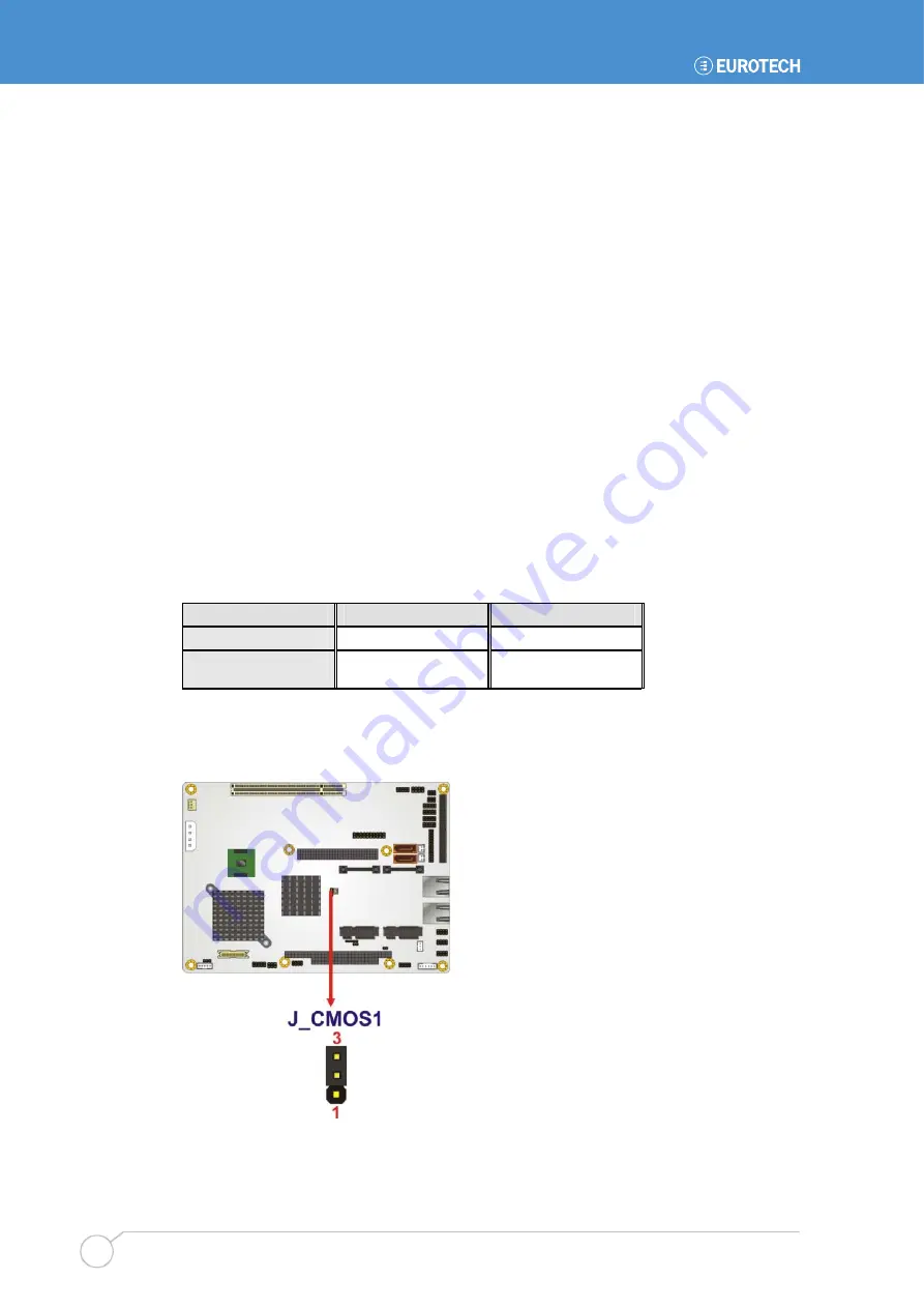
Clear CMOS Jumper 

Jumper Label: 

J_CMOS1


Jumper Type: 

3-pin header 

Jumper Settings: 

See 

Table 33


Jumper Location: 

See 

Figure 50


If the ALUDRA fails to boot due to improper BIOS settings, the clear CMOS jumper clears 
the CMOS data and resets the system BIOS information. To do this, use the jumper cap 
to close pins 2 and 3 for a few seconds then reinstall the jumper clip back to pins 1 and 2. 

If the “CMOS Settings Wrong” message is displayed during the boot up process, the fault 
may be corrected by pressing the F1 to enter the CMOS Setup menu.  Do one of the 
following: 


Enter the correct CMOS setting 


Load Optimal Defaults 


Load Failsafe Defaults.   

After having done one of the above, save the changes and exit the CMOS Setup menu.  

The clear CMOS jumper settings are shown in 

Table 33

Clear CMOS 

Description 


Short 1 - 2  

Keep CMOS Setup 

Default 

Short 2 - 3 

Clear CMOS 
Setup 


Table 33: Clear CMOS Jumper Settings 

The location of the clear CMOS jumper is shown in 

Figure 50 

below. 


Figure 50: Clear CMOS Jumper 

Summary of Contents for ALUDRA

Page 1: ...Issue A November 2009 ETH_ALUDRA_USM DIGITAL TECHNOLOGIES FOR A BETTER WORLD www eurotech com USER MANUAL ALUDRA 5 25 Single Board Computer ...

Page 2: ...ils Disclaimer The information in this document is subject to change without notice and should not be construed as a commitment by any Eurotech company While reasonable precautions have been taken Eurotech assumes no responsibility for any error that may appear in this document Trademarks All trademarks both marked and not marked appearing in this document are the property of their respective owne...

Page 3: ...l Peripheral Interface Connector Panel 58 Installation 59 Installation Considerations 59 SO DIMM and CF Card Installation 61 Jumper Settings 63 Chassis Installation 70 Internal Peripheral Device Connections 71 External Peripheral Interface Connection 76 AMI BIOS 77 Main 79 Advanced 80 PCI PnP 101 Boot 103 Security 105 Chipset 106 Exit 110 Appendix A Terminology 111 Appendix B DIO Interface 113 DIO...

Page 4: ...rvice and repair of this equipment Failure to comply with these precautions or with specific warnings elsewhere in this manual violates safety standards of design manufacture and intended use of the equipment Eurotech assumes no liability for the customer s failure to comply with these requirements The safety precautions listed below represent warnings of certain dangers of which Eurotech is aware...

Page 5: ...e warnings are not carefully followed Appropriate safety precautions should always be used these should meet the requirements set out for the environment that the equipment will be deployed in Battery The board contains a lithium non rechargeable battery Do not short circuit the battery or place on a metal surface where the battery terminals could be shorted When disposing of the board or battery ...

Page 6: ...August 13th 2005 and implies that you must separate all of its components when possible and dispose of them in accordance with local waste disposal legislations Because of the substances present in the equipment improper use or disposal of the refuse can cause damage to human health and to the environment With reference to WEEE it is compulsory not dispose of the equipment with normal urban refuse...

Page 7: ...FSB and a 512 KB L2 cache The ALUDRA also supports one 200 pin 533MHz 2 0GB max DDR2 SDRAM SO DIMM The board comes with one LVDS connector and supports 18 bit dual channel LVDS screens The ALUDRA also comes with one PCI socket two PCI Express PCIe sockets a PC 104 Plus expansion slot and two Gigabit Ethernet GbE connectors Figure 1 ALUDRA ...

Page 8: ...RA at a glance The ALUDRA has a wide variety of peripheral interface connectors Figure 2 is a labelled photo of the peripheral interface connectors on the ALUDRA Figure 2 ALUDRA Overview Front View Figure 3 ALUDRA Overview Solder Side ...

Page 9: ...nectors 44 pin One Infrared interface IrDA connector One Keyboard mouse connector One LVDS connector One Parallel port connector One PC 104 Plus slot One PCI slot Two PCIe Mini Card slots Two Gigabit Ethernet GbE connectors Two Serial ATA SATA drive connectors One SDVO connector Three RS 232 serial port connectors One RS 232 422 485 serial port connector One TPM connector One TV Out connector Thre...

Page 10: ...tek RTL8111CP GbE controllers COM Three RS 232 serial ports One RS 232 422 485 serial port USB2 0 Six USB 2 0 devices supported by on board pin headers SATA Two 1 5 Gbps SATA drives supported Keyboard mouse One 6 pin header for keyboard and mouse Parallel Port One 26 pin parallel port connector Hard Drives One 44 pin IDE connector connects to two Ultra ATA33 66 100 devices TPM One 20 pin header su...

Page 11: ...pported Power Consumption 5V 2 89A 12V 0 04A 1 6 GHz Intel Atom N270 CPU with one 1 GB DDR2 SO DIMM Temperature 0ºC 60ºC 32ºF 140ºF Humidity operating 5 95 non condensing Dimensions LxW 203 mm x 146 mm Weight GW NW 1000g 400g Table 1 Technical Specifications ...

Page 12: ...ALUDRA user manual Issue A 12 Detailed Specifications Board Dimensions The dimensions of the board are listed below Length 203 mm Width 146 mm Figure 4 ALUDRA Dimensions mm ...

Page 13: ...nector panel dimensions are shown in Figure 5 Figure 5 External Interface Panel Dimensions mm Data Flow Figure 6 shows the data flow between the two on board chipsets and other components installed on the motherboard and described in the following sections of this chapter Figure 6 Data Flow Block Diagram ...

Page 14: ... cache and 24 kB write back data cache 533 MHz source synchronous front side bus FSB 2 Threads support On die 512 kB 8 way L2 cache Support for IA 32 bit architecture Intel Streaming SIMD Extensions 2 and 3 Intel SSE2 and Intel SSE3 support and Supplemental Streaming SIMD Extension 3 SSSE3 support Micro FCBGA8 packaging technologies Thermal management support via Intel Thermal Monitor 1 and Intel ...

Page 15: ...pecifications Issue A 15 Front Side Bus FSB The Intel Atom processor on the ALUDRA is interfaced to the Intel 945GSE through a 533 MHz front side bus FSB The FSB is shown in Figure 8 below Figure 8 Front Side Bus ...

Page 16: ...d mode of operation Enhanced Addressing support Swap only The SO DIMM socket is shown in Figure 9 below Figure 9 DDR2 SO DIMM Socket Intel 945GSE Graphics The Intel 945GSE supports CRT LVDS TV Out and SDVO The internal graphics engine has the following features Intel Gen 3 5 Integrated Graphics Engine 250 MHz core render clock and 200 MHz core display clock at 1 05 V core voltage Supports TV Out L...

Page 17: ...es Integrated 400 MHz RAMDAC Analogue Monitor Support up to QXGA Support for CRT Hot Plug LVDS Interface The LVDS interface is connected directly to the LVDS connector on the board Figure 10 The LVDS interface has the following features Panel support up to UXGA 1600 x 1200 25 MHz to 112 MHz single dual channel 18 bpp TFT panel type supported Pixel Dithering for 18 bit TFT panel to emulate 24 bpp t...

Page 18: ...Issue A 18 TV Out Interface The TV Out interface Figure 10 has the following features Three integrated 10 bit DACS Overscaling NTSC PAL Component S Video and Composite Output interfaces HDTV support 480p 720p 1080i 1080p ...

Page 19: ...CI operations Supports ACPI Power Management Logic Contains Enhanced DMA controller Interrupt controller Timer functions Integrated SATA host controller with DMA operations interfaced to two SATA connectors on the ALUDRA Supports the four USB 2 0 devices on the ALUDRA with four UHCI controllers and one EHCI controller Complies with System Management Bus SMBus Specification Version 2 0 Supports Aud...

Page 20: ...me of the features of the RealTek ALC655 are listed below Meets performance requirements for audio on PC99 2001 systems Meets Microsoft WHQL WLP 2 0 audio requirements 16 bit Stereo full duplex CODEC with 48KHz sampling rate Compliant with AC 97 Rev 2 3 specifications Front Out Surround Out MIC In and LINE In Jack Sensing 14 318MHz 24 576MHz PLL to eliminate crystal 12 288MHz BITCLK input Integrat...

Page 21: ...Ds Ultra ATA 100 with data transfer rates up to 100MB s Ultra ATA 66 with data transfer rates up to 66MB s Specification Ultra ATA 100 Ultra ATA 66 IDE devices 2 2 PIO Mode 0 4 0 4 PIO Max Transfer Rate 16 6 MB s 16 6 MB s DMA UDMA designation UDMA 3 4 UDMA 3 4 DMA UDMA Max Transfer 100MB s 66MB s Controller Interface 5V 5V Table 2 Supported HDD Specifications Intel ICH7 M Low Pin Count LPC Interf...

Page 22: ...vision 2 3 implementation Some of the features of the PCI interface are listed below PCI Revision 2 3 compliant 33MHz 5V tolerant PCI signals except PME Integrated PCI arbiter supports up to seven PCI bus masters The PCI bus is connected to a PC 104 Plus connector as shown in Figure 13 Figure 13 PC 104 Plus Connector ...

Page 23: ...e signal technology they offer high speed transmission over CAT 5 UTP cable or CAT 3 UTP 10Mbps only cable Functions such as Crossover Detection Auto Correction polarity correction adaptive equalization cross talk cancellation echo cancellation timing recovery and error correction are implemented to provide robust transmission and reception capability at high speeds Some of the features of the Rea...

Page 24: ...Ie Mini Expansion Slots Two PCIe x1 lanes in combination with USB port on the ICH7 M is interfaced directly to two PCIe mini expansion slots These enable the addition of PICe mini expansion devices The PCIe mini slots are shown in Figure 15 Figure 15 PCIe Mini Slots Intel ICH7 M Real Time Clock 256 bytes of battery backed RAM is provided by the Motorola MC146818A real time clock RTC integrated int...

Page 25: ...ives with independent DMA operations Two SATA controllers are connected to two SATA connectors on the ALUDRA The SATA connectors are shown in Figure 16 Figure 16 SATA Connectors SATA controller specifications are listed below Supports four SATA drives Supports 1 5 Gb s data transfer speeds Supports Serial ATA Specification Revision 1 0a ...

Page 26: ...ers of up to 480MB s is enabled with the ICH7 M integrated Enhanced Host Controller Interface EHCI compliant host controller USB full speed and low speed signalling is supported by the ICH7 M integrated Universal Host Controller Interface UHCI controllers The six USB ports implemented on the ALUDRA are connected to three internal connectors See Figure 17 Figure 17 On board USB Implementation ...

Page 27: ... with Environment Controller integration Some of the features of the iTE IT8718F chipset are listed below ACPI and LANDesk Compliant Enhanced Hardware Monitor Fan Speed Controller Two 16C550 UARTs for serial port control One IEEE 1284 Parallel Port Keyboard Controller Watchdog Timer Some of the Super I O features are described in more detail below Super I O LPC Interface The LPC interface on the S...

Page 28: ...d from the BIOS Hardware Health Configuration menu Super I O Fan Speed Controller The Super I O fan speed controller enables the system to monitor the speed of the fan One of the pins on the fan connector is reserved for fan speed detection and interfaced to the fan speed controller on the Super I O The fan speed is then reported in the BIOS Super I O Keyboard Mouse Controller The Super I O keyboa...

Page 29: ... in the BIOS Hardware Health Configuration menu Operating Temperature and Temperature Control The maximum and minimum operating temperatures for the ALUDRA are listed below Minimum Operating Temperature 0ºC 32 F Maximum Operating Temperature 60 C 140 F A heat sink must be installed on the CPU Thermal paste must be smeared on the lower side of the heat sink before it is mounted on the CPU Heat sink...

Page 30: ...ed please follow anti static precautions and make sure the packing box is facing upwards so the ALUDRA does not fall out of the box No cables are provided with the ALUDRA A list of available cables and modules for the ALUDRA can be found in Appendix E Cable Kit and Optional Items page 120 ...

Page 31: ...rs rear panel peripheral connectors and on board jumpers Figure 19 Connector and Jumper Locations Front Side Figure 20 Connector and Jumper Locations Solder Side Table 4 shows a list of the peripheral interface connectors on the ALUDRA Detailed descriptions of these connectors can be found below ...

Page 32: ...lel port connector 26 pin header J3 PCI 104 slot 120 pin socket J4 PC 104 slot 104 pin socket J6 PCIe Mini Card slot PCIe Mini Slot MINI_PCIE1 PCIe Mini Card slot PCIe Mini Slot MINI_PCIE2 SDVO connector 47 pin connector CN3 Serial ATA SATA drive connector 7 pin SATA SATA1 Serial ATA SATA drive connector 7 pin SATA SATA2 SATA power connector 2 pin wafer CN1 SATA power connector 2 pin wafer CN2 RS ...

Page 33: ...ipheral Connectors Internal peripheral connectors are found on the motherboard and are only accessible when the motherboard is outside of the chassis This section has complete descriptions of all the internal peripheral connectors on the ALUDRA AT Power Connector CN Label J2 CN Type 4 pin power connector 1x4 CN Location See Figure 21 CN Pinouts See Table 6 The 4 pin AT power connector is connected...

Page 34: ...enables the ALUDRA to be connected to an ATX power supply In default mode the ALUDRA can only use an AT power supply To enable an ATX power supply the AT Power Select jumper must also be configured See Installation page 59 for more details Figure 22 ATX Power Supply Enable Connector Location PIN NO DESCRIPTION 1 5V Standby 2 GND 3 PS_ON Table 7 ATX Power Supply Enable Connector Pinouts ...

Page 35: ...es including speakers and microphones for the input and output of audio signals to and from the system LIL MICIN LINEOUTR LIR LINEOUTL GND_AUD J8 PIN HEADER 2 5 1 1 2 2 3 3 4 4 5 5 6 6 7 7 9 9 8 8 10 10 Figure 23 Audio Connector Location 9 pin PIN NO DESCRIPTION PIN NO DESCRIPTION 1 LINE_OUTR 2 LIR 3 GND 4 GND 5 LINE_OUTL 6 LIL 7 GND 8 GND 9 MIC_IN 10 NA Table 8 Audio Connector Pinouts 9 pin ...

Page 36: ...re 24 CN Pinouts See Table 9 The backlight inverter connector provides the backlight on the LCD display connected to the ALUDRA with 12V of power Figure 24 Panel Backlight Connector Pinout Locations PIN NO DESCRIPTION 1 LCD Backlight Control PWM 2 GND 3 12V 4 GND 5 Backlight Enable Table 9 Panel Backlight Connector Pinouts ...

Page 37: ...ash Socket CN Label J9 solder side CN Type 50 pin header 2x25 CN Location See Figure 25 CN Pinouts See Table 10 A CF Type II memory card is inserted to the CF socket on the solder side of the ALUDRA Figure 25 CF Card Socket Location ...

Page 38: ... 30 DATA 14 6 DATA 7 31 DATA 15 7 CS0 32 CS1 8 NC 33 NC 9 GND 34 IOR 10 NC 35 IOW 11 NC 36 5V 12 NC 37 IRQ 13 5V 38 5V 14 NC 39 CSEL 15 NC 40 NC 16 NC 41 RESET 17 NC 42 IORDY 18 ADDR2 43 SDREQ 19 ADDR 1 44 SDACK 20 ADDR 0 45 DASP 21 DATA 0 46 PDIAG 22 DATA 1 47 DATA 8 23 DATA 2 48 DATA 9 24 NC 49 DATA 10 25 CARD_DETECT2 50 GND Table 10 CF Card Socket Pinouts ...

Page 39: ...e 11 The 2x5 CRT pin connector provides connectivity to an external VGA port enabling the system to be connected to a standard CRT screen Figure 26 VGA Connector Pinout Locations PIN NO DESCRIPTION PIN NO DESCRIPTION 1 RED 2 DDC_CLK 3 GREEN 4 DDC_DATA 5 BLUE 6 GND 7 HSYNC 8 GND 9 VSYNC 10 GND Table 11 VGA Connector Pinouts ...

Page 40: ...Pinouts See Table 12 The digital input output connector is managed through a Super I O chip The DIO connector pins are user programmable Figure 27 DIO Connector Locations PIN NO DESCRIPTION PIN NO DESCRIPTION 1 GND 2 5V 3 OUTPUT 3 4 OUTPUT 2 5 OUTPUT 1 6 OUTPUT 0 7 INPUT 3 8 INPUT 2 9 INPUT 1 10 INPUT 0 Table 12 DIO Connector Pinouts ...

Page 41: ...a 12V 500mA current to the cooling fan The connector has a rotation pin to get rotation signals from fans and notify the system so the system BIOS can recognize the fan speed Please note that only specified fans can issue the rotation signals Figure 28 12V Fan Connector Location PIN NO DESCRIPTION 1 GND 2 12V 3 Fan Speed Detect PWM Table 13 12V Fan Connector Pinouts ...

Page 42: ...rnal switches and indicators to monitor and controls the motherboard These indicators and switches include Power button Reset Power LED HDD LED Figure 29 Front Panel Connector Pinout Locations 8 pin FUNCTION PIN DESCRIPTION FUNCTION PIN DESCRIPTION 1 PWR_BTN 2 VCC5 Power Button 3 GND Power LED 4 GND 5 HDD_LED 6 SYSRST HDD LED 7 HDD_LED Reset 8 GND Table 14 Front Panel Connector Pinouts 8 pin ...

Page 43: ...pin CN Label IDE1 CN Type 44 pin box header 2x22 CN Location See Figure 30 CN Pinouts See Table 15 One 44 pin IDE device connector on the ALUDRA supports connectivity to two hard disk drives Figure 30 Secondary IDE Device Connector Locations ...

Page 44: ... 4 10 DATA 11 11 DATA 3 12 DATA 12 13 DATA 2 14 DATA 13 15 DATA 1 16 DATA 14 17 DATA 0 18 DATA 15 19 GND 20 NC 21 IDE DREQ 22 GND 23 IOW 24 GND 25 IOR 26 GND 27 IDE CHRDY 28 GND 29 IDE DACK 30 GND 31 INTERRUPT 32 NC 33 SA1 34 NC 35 SA0 36 SA2 37 CS0 38 CS1 39 HDD ACTIVE 40 GND 41 VCC 42 VCC 43 GND 44 NC Table 15 Secondary IDE Connector Pinouts ...

Page 45: ...N Location See Figure 31 CN Pinouts See Table 16 The infrared interface connector supports both Serial Infrared SIR and Amplitude Shift Key Infrared ASKIR interfaces Figure 31 Infrared Connector Pinout Locations PIN NO DESCRIPTION 1 5V 2 NC 3 IR_RX 4 GND 5 IR_TX Table 16 Infrared Connector Pinouts ...

Page 46: ...e Table 17 The keyboard and mouse connector can be connected to a standard PS 2 cable or PS 2 Y cable to add keyboard and mouse functionality to the system Figure 32 Keyboard Mouse Connector Location PIN NO DESCRIPTION 1 2 5V 2 MOUSE DATA 3 MOUSE CLOCK 4 KEYBOARD DATA 5 KEYBOARD CLOCK 6 GND Table 17 Keyboard Mouse Connector Pinouts ...

Page 47: ...nnel 18 bit LVDS panel Figure 33 LVDS LCD Connector Pinout Location PIN NO DESCRIPTION PIN NO DESCRIPTION 1 GND 2 GND 3 LVDSA1 4 LVDSA1 5 LVDSA2 6 LVDSA2 7 LVDSA3 8 LVDSA3 9 LVDSACLK 10 LVDSACLK 11 NC 12 NC 13 GND 14 GND 15 LVDSB1 16 LVDSB1 17 LVDSB2 18 LVDSB2 19 LVDSB3 20 LVDSB3 21 LVDSBCLK 22 LVDSBCLK 23 NC 24 NC 25 GND 26 GND 27 LCDVCC 28 LCDVCC 29 LCDVCC 30 LCDVCC Table 18 LVDS LCD Port Connec...

Page 48: ...rt connector interface or some other parallel port device such as a printer Figure 34 Parallel Port Connector Location PIN NO DESCRIPTION PIN NO DESCRIPTION 1 STROBE 14 AUTOFD 2 DATA 0 15 ERROR 3 DATA 1 16 INIT 4 DATA 2 17 SELIN 5 DATA 3 18 GND 6 DATA 4 19 GND 7 DATA 5 20 GND 8 DATA 6 21 GND 9 DATA 7 22 GND 10 ACK 23 GND 11 BUSY 24 GND 12 PE 25 GND 13 SEL 26 GND Table 19 Parallel Port Connector Pi...

Page 49: ...or CN Label CN3 CN Type 47 pin connector 1x47 CN Location See Figure 35 CN Pinouts See Table 20 The SDVO Serial Digital Video Out port B connector supports additional video signalling interfaces Figure 35 SDVO Connector Pinout Locations ...

Page 50: ...D 7 GND 31 GND 8 SDVOB_CLK 32 SDVO1_STALL 9 SDVOB_ CLK 33 SDVO1_STALL 10 GND 34 GND 11 SDVOB_GREEN 35 SDVO_TVCLKIN 12 SDVOB_GREEN 36 SDVO_TVCLKIN 13 GND 37 GND 14 SDVOC_INT 38 SDVO_CLK 15 SDVOC_INT 39 SDVO_DATA 16 GND 40 PCIRST 17 SDVOB_INT 41 5VS 18 SDVOB_INT 42 5VS 19 GND 43 5VS 20 SDVOC_BLUE 44 NC 21 SDVOC_BLUE 45 NC 22 GND 46 GND 23 SDVOC_RED 47 GND 24 SDVOC_RED Table 20 SDVO Connector Pinouts...

Page 51: ... 21 The two SATA drive connectors are each connected to a first generation SATA drive First generation SATA drives transfer data at speeds as high as 150 Mb s The SATA drives can be configured in a RAID configuration Figure 36 SATA Drive Connector Locations PIN NO DESCRIPTION 1 GND 2 TX 3 TX 4 GND 5 RX 6 RX 7 GND Table 21 SATA Drive Connector Pinouts ...

Page 52: ...Label CN1 and CN2 CN Type 2 pin wafer CN Location See Figure 37 CN Pinouts See Table 22 The SATA power connector provides 5V power to the SATA drive Figure 37 SATA Power Connector Locations PIN NO DESCRIPTION 1 5V 2 GND Table 22 SATA Power Connector Pinouts ...

Page 53: ...uts See Table 23 The 10 pin serial port connector provides a RS 232 serial communications channel The COM serial port connectors can be connected to external RS 232 serial port devices Figure 38 COM Connector Pinout Locations PIN NO DESCRIPTION PIN NO DESCRIPTION 1 DCD 2 DSR 3 RX 4 RTS 5 TX 6 CTS 7 DTR 8 RI 9 GND 10 NC Table 23 COM Connector Pinouts ...

Page 54: ...d jumper refer to COM 3 Function Select Jumper page 67 The JP2 connector provides the RS 422 or RS 485 signals when COM 3 is set for RS 422 or RS 485 devices TX_422 TX_422 RX3 RX3 JP2 HEADER_2X3_2 1 2 3 4 5 6 D D Figure 39 COM 3 RS 422 485 Connector Pinout Locations PIN NO DESCRIPTION PIN NO DESCRIPTION 1 RS422_TX 2 RS422_RX 3 RS422_TX 4 RS422_RX 5 RS485_DATA 6 RS485_DATA Table 24 COM 3 RS 422 485...

Page 55: ...Table 25 The Trusted Platform Module TPM connector secures the system on bootup Figure 40 TPM Connector Pinout Locations PIN NO DESCRIPTION PIN NO DESCRIPTION 1 CLK 2 GND 3 FRAME 4 KEY 5 RESET 6 5V 7 ADDR 3 8 ADDR2 9 3 3V 10 ADDR 1 11 ADDR 0 12 GND 13 SCL 14 SDA 15 SB3V 16 SERIRQ 17 GND 18 GLKRUN 19 PCPD 20 DREQ Table 25 TPM Connector Pinouts ...

Page 56: ... connector connects to a TV output by using an S Video or RCA connector The TV out connector makes displaying media data on a television easier Figure 41 TV Connector Pinout Locations S Video Connector PIN NO DESCRIPTION PIN NO DESCRIPTION 1 GND 2 GREEN Y 3 GND 4 RED C RCA Connector only video signal 5 GND 6 BLUE CVBS Table 26 TV Port Connector Pinouts ...

Page 57: ... each provide connectivity to two USB 1 1 or two USB 2 0 ports Each USB connector can support two USB devices Additional external USB ports are found on the rear panel The USB ports are used for I O bus expansion Figure 42 USB Connector Pinout Locations PIN NO DESCRIPTION PIN NO DESCRIPTION 1 5V 2 GND 3 DATA 4 DATA 5 DATA 6 DATA 7 GND 8 5V Table 27 USB Port Connector Pinouts ...

Page 58: ...trollers The controllers can connect to the LAN through two RJ 45 LAN connectors There are two LEDs on the connector indicating the status of LAN The pin assignments are listed in the following table PIN DESCRIPTION PIN DESCRIPTION 1 TX 5 CT_TERM 2 TX 6 RX 3 RX 7 CT_TERM 4 CT_TERM 8 CT_TERM Table 28 LAN Pinouts Figure 44 RJ 45 Ethernet Connector The RJ 45 Ethernet connector has two status LEDs one...

Page 59: ...ic components are easily damaged by ESD Wearing an ESD cuff removes ESD from the body and helps prevent ESD damage Place the ALUDRA on an antistatic pad When installing or configuring the motherboard place it on an antistatic pad This helps to prevent potential ESD damage Turn all power to the ALUDRA off When working with the ALUDRA make sure that it is disconnected from all power supplies and tha...

Page 60: ...wer supply is being used The following devices are properly connected Primary and secondary IDE device SATA drives Power supply USB cable Serial port cable The following external peripheral devices are properly connected to the chassis VGA screen Keyboard Mouse RS 232 serial communications device USB devices ...

Page 61: ...DIMM socket Place the ALUDRA on an anti static pad with the solder side facing up 2 Align the SO DIMM with the socket The SO DIMM must be oriented in such a way that the notch in the middle of the SO DIMM must be aligned with the plastic bridge in the socket 3 Insert the SO DIMM Push the SO DIMM chip into the socket at an angle See Figure 45 4 Open the SO DIMM socket arms Gently pull the arms of t...

Page 62: ...w the steps below 1 Locate the CF card socket Place the ALUDRA on an anti static pad with the solder side facing up Locate the CF card 2 Align the CF card Make sure the CF card is properly aligned with the CF socket 3 Insert the CF card Gently insert the CF card into the socket making sure the socket pins are properly inserted into the socket See Figure 46 Figure 46 CF Card Installation ...

Page 63: ...d to OPEN a jumper means removing the plastic clip from a jumper Figure 47 Jumper Locations Before the ALUDRA is installed in the system the jumpers must be set in accordance with the desired configuration The jumpers on the ALUDRA are listed in Table 30 Description Label Type AT Power Mode Setting ATXCTL1 2 pin header CF Card Setting J_CF1 2 pin header Clear CMOS J_CMOS1 3 pin header COM3 Functio...

Page 64: ...ure 48 The AT Power Select jumper specifies the systems power mode as AT or ATX AT Power Select jumper settings are shown in Table 31 AT Power Select Description Open Use ATX power Default Short Use AT power Table 31 AT Power Select Jumper Settings The location of the AT Power Select jumper is shown in Figure 48 below Figure 48 AT Power Select Jumper Location ...

Page 65: ...d Setup jumper sets the CF Type I card or CF Type II cards as either the slave device or the master device CF Card Setup jumper settings are shown in Table 32 CF Card Setup Description Open Slave Default Closed Master Table 32 CF Card Setup Jumper Settings The CF Card Setup jumper location is shown in Figure 49 Figure 49 CF Card Setup Jumper Location ...

Page 66: ...s 1 and 2 If the CMOS Settings Wrong message is displayed during the boot up process the fault may be corrected by pressing the F1 to enter the CMOS Setup menu Do one of the following Enter the correct CMOS setting Load Optimal Defaults Load Failsafe Defaults After having done one of the above save the changes and exit the CMOS Setup menu The clear CMOS jumper settings are shown in Table 33 Clear ...

Page 67: ...ication protocol used by the third serial communications port COM 3 as RS 232 RS 422 or RS 485 The COM 3 Function Select settings are shown in Table 34 COM 3 Function Select Description Short 1 2 RS 232 Default Short 3 4 RS 422 Short 5 6 RS 485 Table 34 COM 3 Function Select Jumper Settings The COM 3 Function Select jumper location is shown in Figure 51 Figure 51 COM 3 Function Select Jumper Locat...

Page 68: ...d The LVDS Panel Resolution jumper settings are shown in Table 35 J_LCD_TYPE1 Description Open 640 x 480 18 bit Short 1 2 800 x 480 18 bit Short 3 4 800 x 600 18 bit Short 1 2 3 4 1024 X 768 18 bit Short 5 6 1280X1024 36 bit Short 1 2 5 6 1400 X 1050 36 bit Short 3 4 5 6 1400 x 900 36 bit Short 1 2 3 4 5 6 1600 x 1200 36 bit Table 35 LVDS Panel Resolution Jumper Settings The LVDS Panel Resolution ...

Page 69: ... Location See Figure 53 The LVDS Voltage Selection jumpers allow the LVDS screen voltages to be set J_VLVDS1 sets the voltage connected to LVDS1 and J_VLVDS2 sets the voltage for the screen connected to LVDS2 The LVDS Voltage Selection jumper settings are shown in Table 36 LCD Voltage Select Description Short 1 2 3 3V LVDS Default Short 2 3 5V LVDS Table 36 LVDS Voltage Selection Jumper Settings T...

Page 70: ...avel through the heat sink surface In a system with an individual power supply unit the cooling fan of a power supply can also help generate airflow through the board surface Eurotech has a wide range of backplanes available Please contact a Eurotech sales representative or visit the Eurotech website to find out more about the available chassis See Eurotech Group Worldwide Presence page 122 for co...

Page 71: ...Line In and Line Out connect to two speakers To install the audio kit please refer to the steps below 1 Locate the audio connector The location of the 10 pin audio connector is shown in Connectors page 31 2 Align pin 1 Align pin 1 on the on board connector with pin 1 of the audio kit connector Pin 1 of the audio kit connector is indicated with a white dot Figure 54 Audio Kit Cable Connection 3 Con...

Page 72: ...55 3 Insert the cable connectors Once the cable connector is properly aligned with the keyboard mouse connector on the ALUDRA connect the cable connector to the on board connectors See Figure 55 Figure 55 Keyboard mouse Y cable Connection 4 Attach PS 2 connectors to the chassis The keyboard mouse Y cable connector is connected to two PS 2 connectors To secure the PS 2 connectors to the chassis ple...

Page 73: ... page 31 2 Insert the cable connector Insert the connector into the serial port box header See Figure 56 The red wire in the RS232 cable indicates pin 1 Align pin 1 of the on board connector with pin 1 of the RS232 cable connector Figure 56 Single RS 232 Cable Installation 3 Secure the bracket The RS 232 connector has two retention screws that must be secured to a chassis or bracket 4 Connect the ...

Page 74: ...lip on the connector at the end of the SATA cable and insert the cable connector into the on board SATA drive connector See Figure 57 Figure 57 SATA Drive Cable Connection 3 Connect the cable to the SATA disk Connect the connector on the other end of the cable to the connector at the back of the SATA drive See Figure 58 4 Connect the SATA power cable Connect the SATA power connector to the back of...

Page 75: ...wo connectors Correctly align pin 1on each cable connector with pin 1 on the ALUDRA USB connector 3 Insert the cable connectors Once the cable connectors are properly aligned with the USB connectors on the ALUDRA connect the cable connectors to the on board connectors See Figure 59 Figure 59 Dual USB Cable Connection 4 Attach the USB connectors to the chassis The USB 2 0 connectors have two retent...

Page 76: ...ngle Connector There are two external RJ 45 LAN connectors The RJ 45 connectors enable connection to an external network To connect a LAN cable with an RJ 45 connector please follow the instructions below 1 Locate the RJ 45 connectors The locations of the USB connectors are shown in Connectors page 31 2 Align the connectors Align the RJ 45 connector on the LAN cable with one of the RJ 45 connector...

Page 77: ...hange entries press F1 for help and press ESC to quit Navigation keys are shown in Key Function Up arrow Move to previous item Down arrow Move to next item Left arrow Move to the item on the left hand side Right arrow Move to the item on the right hand side Esc key Main Menu Quit and not save changes into CMOS Status Page Setup Menu and Option Page Setup Menu Exit current page and return to Main M...

Page 78: ...ems Main Changes the basic system configuration Advanced Changes the advanced system settings PCIPnP Changes the advanced PCI PnP Settings Boot Changes the system boot configuration Security Sets User and Supervisor Passwords Chipset Changes the chipset settings Power Changes power management settings Exit Selects exit options and loads default settings The following sections completely describe t...

Page 79: ...rrent BIOS version Build Date Date the current BIOS version was made ID Installed BIOS ID Processor Displays auto detected CPU specifications Type Names the currently installed processor Speed Lists the processor speed Count The number of CPUs on the motherboard System Memory Displays the auto detected system memory Size Lists memory size The System Overview field also has two user configurable fi...

Page 80: ... the sections below may cause the system to malfunction Make sure that the settings made are compatible with the hardware CPU Configuration page 81 IDE Configuration page 82 SuperIO Configuration page 87 Hardware Health Configuration page 91 Power Configuration page 93 Remote Access Configuration page 96 USB Configuration page 98 Trusted Computing page 99 BIOS Menu 2 Advanced ...

Page 81: ...enu 3 CPU Configuration The CPU Configuration menu BIOS Menu 3 lists the following CPU details Manufacturer Lists the name of the CPU manufacturer Brand String Lists the brand name of the CPU being used Frequency Lists the CPU processing speed FSB Speed Lists the FSB speed Cache L1 Lists the CPU L1 cache size Cache L2 Lists the CPU L2 cache size ...

Page 82: ...re the ATA IDE controller Disabled Disables the on board ATA IDE controller Compatible DEFAULT Configures the on board ATA IDE controller to be in compatible mode In this mode a SATA channel will replace one of the IDE channels This mode supports up to 4 storage devices Enhanced Configures the on board ATA IDE controller to be in Enhanced mode In this mode IDE channels and SATA channels are separa...

Page 83: ...ed IDE devices The following IDE devices are detected and are shown in the IDE Configuration menu Primary IDE Master Primary IDE Slave Secondary IDE Master Secondary IDE Slave The IDE Configuration menu BIOS Menu 4 allows changes to the configurations for the IDE devices installed in the system If an IDE device is detected and one of the above listed four BIOS configuration options are selected th...

Page 84: ...e installed device Async DMA Indicates the highest Asynchronous DMA Mode that is supported Ultra DMA Indicates the highest Synchronous DMA Mode that is supported S M A R T Indicates whether or not the Self Monitoring Analysis and Reporting Technology protocol is supported 32Bit Data Transfer Enables 32 bit data transfer Type Auto Use the Type BIOS option select the type of device the AMIBIOS attem...

Page 85: ...or Transfer support on the drive on the specified channel If supported the data transfer to and from the device occurs multiple sectors at a time PIO Mode Auto Use the PIO Mode option to select the IDE PIO Programmable I O mode program timing cycles between the IDE drive and the programmable IDE controller As the PIO mode increases the cycle time decreases Auto DEFAULT BIOS auto detects the PIO mo...

Page 86: ...DMA mode 1 selected with a maximum data transfer rate of 25MBps UDMA2 Ultra DMA mode 2 selected with a maximum data transfer rate of 33 3MBps UDMA3 Ultra DMA mode 3 selected with a maximum data transfer rate of 44MBps To use this mode it is required that an 80 conductor ATA cable is used UDMA4 Ultra DMA mode 4 selected with a maximum data transfer rate of 66 6MBps To use this mode it is required t...

Page 87: ...IO Configuration Use the Super IO Configuration menu BIOS Menu 6 to set or change the configurations for the FDD controllers parallel ports and serial ports BIOS Menu 6 Super IO Configuration Parallel Port Address 378 Use the Parallel Port Address option to select the parallel port base address Disabled No base address is assigned to the Parallel Port 378 DEFAULT Parallel Port I O port address is ...

Page 88: ...em and the parallel port device and the transmission rates between the two are much faster than the Normal mode The parallel port is also be compatible with EPP devices described above Parallel Port IRQ IRQ7 Use the Parallel Port IRQ selection to set the parallel port interrupt address IRQ5 IRQ5 is assigned as the parallel port interrupt address IRQ7 DEFAULT IRQ7 is assigned as the parallel port i...

Page 89: ...3E8 IRQ4 Serial Port 2 I O port address is 3E8 and the interrupt address is IRQ4 2E8 IRQ3 Serial Port 2 I O port address is 2E8 and the interrupt address is IRQ3 Serial Port2 Mode Normal Use the Serial Port2 Mode option to select the Serial Port2 operational mode Normal DEFAULT Serial Port 2 mode is normal IrDA Serial Port 2 mode is IrDA ASK IR Serial Port 2 mode is ASK IR Serial Port3 Address 3E8...

Page 90: ... 232 RS422 RS485 Serial Port 2 signaling mode is RS 422 or RS 485 Serial Port4 Address 2E8 Use the Serial Port4 IRQ option to select the interrupt address for serial port 4 Disabled No base address is assigned to serial port 3 3E8 Serial port 4 I O port address is 3E8 2E8 DEFAULT Serial port 4 I O port address is 2E8 2F0 Serial port 4 I O port address is 2F0 2E0 Serial port 4 I O port address is 2...

Page 91: ...second fan Full On Mode DEFAULT Fan is on all the time Automatic mode Fan is off when the temperature is low enough Parameters must be set by the user PWM Manual mode Pulse width modulation set manually When the CPU FAN Mode Setting option is in the Automatic Mode the following parameters can be set CPU Temp Limit of OFF CPU Temp Limit of Start CPU Fan Start PWM Slope PWM 1 When the CPU FAN Mode S...

Page 92: ...ng fan should automatically turn on When the fan starts it rotates using the starting pulse width modulation PWM specified in the Fan 3 Start PWM option below To select a value select the CPU Temp Limit of Start option and enter a decimal number between 000 and 127 The temperature range is specified below Minimum Value 0 C Maximum Value 127 C CPU Fan Start PWM 070 The Fan 3 Start PWM option can on...

Page 93: ...onitored CPU Temperature System Temperature Fan Speeds The CPU cooling fan speed is monitored CPU Fan Speed Voltages The following system voltages are monitored CPU Core 1 05V 3 30V 5 00V 12 0 V 1 5V 1 8V 5VSB VBAT Power Configuration The Power Configuration menu BIOS Menu 8 configures the Advanced Configuration and Power Interface ACPI and Power Management APM options BIOS Menu 8 Power Configurat...

Page 94: ...tem returns to if there is a sudden loss of power to the system Power Off The system remains turned off Power On The system turns on Last State DEFAULT The system returns to its previous state If it was on it turns itself on If it was off it remains off Power Button Mode On Off Use the Power Button Mode BIOS to specify how the power button functions On Off DEFAULT When the power button is pressed ...

Page 95: ...n a modem Disabled DEFAULT Wake event not generated by an incoming call Enabled Wake event generated by an incoming call Resume on PCI Express WAKE Disabled Use the Resume PCI Express WAKE BIOS option to enable activity on the PCI Express WAKE signal to rouse the system from a suspend or standby state Disabled DEFAULT Wake event not generated by PCI Express WAKE signal activity Enabled Wake event ...

Page 96: ... to display and configure the BIOS settings BIOS Menu 10 Remote Access Configuration Advanced Remote Access Disabled Use the Remote Access option to enable or disable access to the remote functionalities of the system Disabled DEFAULT Remote access is disabled Enabled Remote access configuration options shown below appear Serial Port Number Serial Port Mode Redirection after BIOS POST Terminal Typ...

Page 97: ... the serial port listed above Serial Port Mode 115200 8 n 1 Use the Serial Port Mode option to select baud rate through which the console redirection is made The following configuration options are available 115200 8 n 1 DEFAULT 57600 8 n 1 38400 8 n 1 19200 8 n 1 09600 8 n 1 Identical baud rate setting musts be set on the host a management computer running a terminal software and the slave Redire...

Page 98: ...B Configuration menu BIOS Menu 11 to read USB configuration information and configure the USB settings BIOS Menu 11 USB Configuration USB Functions Enabled Use the USB Function option to enable or disable the USB controllers Disabled USB controllers are enabled Enabled DEFAULT USB controllers are disabled USB 2 0 Controller Enabled The USB 2 0 Controller BIOS option enables or disables the USB 2 0...

Page 99: ...s no USB driver loaded onto the system Disabled Legacy USB support disabled Enabled DEFAULT Legacy USB support enabled Auto Legacy USB support disabled if no USB devices are connected USB2 0 Controller Mode HiSpeed The USB2 0 Controller Mode BIOS option sets the speed of the USB2 0 controller FullSpeed The controller is capable of operating at full speed 12 Mb s HiSpeed DEFAULT The controller is c...

Page 100: ...ALUDRA user manual Issue A 100 TCG TPM Support No Use the TCG TPM Support option to configure support for the TPM No DEFAULT TPM support is disabled Yes TPM support is enabled ...

Page 101: ... system to malfunction BIOS Menu 13 PCI PnP Configuration IRQ Available Use the IRQ address to specify what IRQs can be assigned to a particular peripheral device Available DEFAULT The specified IRQ is available to be used by PCI PnP devices Reserved The specified IRQ is reserved for use by Legacy ISA devices Available IRQ addresses are IRQ3 IRQ4 IRQ5 IRQ7 IRQ9 IRQ10 IRQ 11 IRQ 14 IRQ 15 ...

Page 102: ...fic DMA channel to a particular PCI PnP device Available DEFAULT The specified DMA is available to be used by PCI PnP devices Reserved The specified DMA is reserved for use by Legacy ISA devices Available DMA Channels are DM Channel 0 DM Channel 1 DM Channel 3 DM Channel 5 DM Channel 6 DM Channel 7 ...

Page 103: ...oot menu BIOS Menu 14 to configure system boot options BIOS Menu 14 Boot Boot Settings Configuration Use the Boot Settings Configuration menu BIOS Menu 15 to configure advanced system boot options BIOS Menu 15 Boot Settings Configuration ...

Page 104: ...y the information during system boot Bootup Num Lock On The Bootup Num Lock BIOS option allows the Number Lock setting to be modified during boot up Off Does not enable the keyboard Number Lock automatically To use the 10 keys on the keyboard press the Number Lock key located on the upper left hand corner of the 10 key pad The Number Lock LED on the keyboard lights up when the Number Lock is engag...

Page 105: ...talled If a supervisor password must be installed select this field and enter the password After the password has been added Install appears next to Change Supervisor Password Change User Password Use the Change User Password to set or change a user password The default for this option is Not Installed If a user password must be installed select this field and enter the password After the password...

Page 106: ...et Use the Chipset menu BIOS Menu 17 to access the NorthBridge and SouthBridge configuration menus Setting the wrong values for the Chipset BIOS selections in the Chipset BIOS menu may cause the system to malfunction BIOS Menu 17 Chipset ...

Page 107: ... properly If an older ISA expansion card is used please refer to the documentation that came with the card to see if it is necessary to reserve the space Disabled DEFAULT Memory is not reserved for ISA expansion cards Enabled Memory is reserved for ISA expansion cards Internal Graphics Mode Select Enable 8MB The Internal Graphic Mode Select option determines the amount of system memory that can be...

Page 108: ...ved as graphics memory DVMT Mode DEFAULT Graphics memory is dynamically allocated according to the system and graphics needs Combo Mode A fixed portion of graphics memory is reserved as graphics memory If more memory is needed graphics memory is dynamically allocated according to the system and graphics needs DVMT FIXED Memory 128MB Use the DVMT FIXED Memory option to specify the maximum amount of...

Page 109: ...troller is enabled All Disabled DEFAULT The on board audio controller is disabled Spread Spectrum Disabled Use the Spread Spectrum option to reduce the EMI Excess EMI is generated when the system clock generator pulses have extreme values Spreading the pulse spectrum modulates changes in the extreme values from spikes to flat curves thus reducing the EMI This benefit may in some cases be outweighe...

Page 110: ...Exit option to exit the BIOS configuration setup program without saving the changes made to the system Discard Changes Use the Discard Changes option to discard the changes and remain in the BIOS configuration setup program Load Optimal Defaults Use the Load Optimal Defaults option to load the optimal default values for each of the parameters on the Setup menus F9 key can be used for this operatio...

Page 111: ...igured by the end user CODEC The Compressor Decompressor CODEC encodes and decodes digital audio data on the system CMOS Complimentary metal oxide conductor is a type of integrated circuit used in chips like static RAM and microprocessors COM COM is used to refer to serial ports Serial ports offer serial communication to expansion devices The serial port on a personal computer is usually a male DE...

Page 112: ...nt Array of Inexpensive Disks RAID refers to redundantly backing up data on multiple disks to ensure that if one disk fails the data is not lost and can be restored from the remaining disks in the array RAM Random Access Memory RAM is a form of storage used in computer RAM is volatile memory so it loses its data when power is lost RAM has very fast data transfer rates compared to other storage lik...

Page 113: ...ption 1 GND NA NA 2 VCC NA NA 3 Output 3 GP23 General Purpose I O Port 2 Bit 3 4 Output 2 GP22 General Purpose I O Port 2 Bit 2 5 Output 1 GP21 General Purpose I O Port 2 Bit 1 6 Output 0 GP20 General Purpose I O Port 2 Bit 0 7 Input 3 GP33 General Purpose I O 33 8 Input 2 GP32 General Purpose I O 32 9 Input 1 GP31 General Purpose I O 31 10 Input 0 GP30 General Purpose I O 30 Assembly Language Sam...

Page 114: ...state A BIOS function call INT 15H is used to control the Watchdog Timer INT 15H AH 6FH Sub function AL 2 Sets the Watchdog Timer s period BL Time out value Its unit second is dependent on the item Watchdog Timer unit select in CMOS setup Table AH 6FH Sub function Call sub function 2 to set the time out period of Watchdog Timer first If the time out value is not zero the Watchdog Timer starts coun...

Page 115: ...IOD COUNTER W_LOOP MOV AX 6F02H setting the time out value MOV BL 30 time out value is 48 seconds INT 15H ADD THE APPLICATION PROGRAM HERE CMP EXIT_AP 1 is the application over JNE W_LOOP No restart the application MOV AX 6F02H disable Watchdog Timer MOV BL 0 INT 15H EXIT ...

Page 116: ...ALUDRA user manual Issue A 116 Appendix D Address Mapping I O Address Map ...

Page 117: ...Appendix D Address Mapping Issue A 117 Table IO Address Map ...

Page 118: ...ALUDRA user manual Issue A 118 IRQ Address Map Table IRQ Address Map ...

Page 119: ...Appendix D Address Mapping Issue A 119 Memory Address Map Table Memory Address Map ...

Page 120: ...the ALUDRA Item and Part Number Image VGA cable Audio cable KB MS PS 2 Y cable Dual USB cable w o bracket SATA cable RS 232 cable w o bracket Mini jumper pack 2 0mm Eurotech can provide the following optional items for the ALUDRA Item and Part Number Image SATA power cable HDD cable LPT cable w o bracket RS 422 485 cable ...

Page 121: ...02 11 b g PCIe mini card wireless LAN module 802 11b g USB embedded module 20 pin WINBOND TPM module and S W management Tool Please contact a Eurotech sales representative to obtain the cable kit and optional items For contact details see Eurotech Group Worldwide Presence page 122 ...

Page 122: ...tel 44 0 1223 403410 fax 44 0 1223 410457 e mail sales uk eurotech com e mail support uk eurotech com www eurotech com EUROTECH France tel 33 04 72 89 00 90 fax 33 04 78 70 08 24 e mail sales fr eurotech com e mail support fr eurotech com www eurotech com Northern Eastern Europe EUROTECH Finland tel 358 9 477 888 0 fax 358 9 477 888 99 e mail sales fi eurotech com e mail support fi eurotech com ww...

Page 123: ...www eurotech com ...

Reviews: