
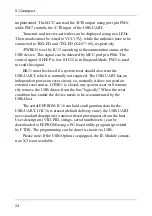


A/D-Converter (ADC)
The S12compact can be equipped with a high-resolution A/D-Con-
verter (ADC). While the on-chip ATD modules of the HCS12 provide
sufficient resolution (10-bit) for a wide range of industrial applications,
the external ADC system on the S12compact provides enhanced
accuracy, which is suitable for measuring devices and data loggers.
The ADS8344 (IC11) from Burr Brown is an 8-channel 16-bit
ADC with serial interface and a conversion rate of up to 100ksps. It is
connected to the SPI-port SPI0 of the MCU. /SPICS2 is the chip select
signal for the ADC (delivered by IC4).
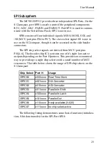
IC10 is a precision voltage reference, delivering 4.096V for the
ADC and the DAC on the S12compact. This reference voltage determi-
nes the maximum limit for the analog inputs AIN0..AIN7. The lower
limit is ground (0V). After opening solder bridge BR9, an external
reference voltage can be used instead of IC10 (note: influence on DAC
IC12). The analog inputs AIN0 to AIN7 as well as the analog supply
voltages (VCCA, VREF, GNDA) are available at connector X4.
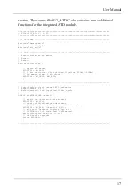
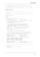
The following software example for the ADS8344 uses the basic
SPI functions (shown above).
//-----------------------------------------------------------------------------
// Note: CPHA=0, CPOL=0 required
// clock rate max. 2MHz
// conversion takes max. 8µs
//
UINT16 getADS8344(UINT8 channel) {
volatile UINT8 n;
UINT16 adcresult;
// set up SPI mode
SPI0CR1 = BM_SPE | BM_MSTR; // CPOL=0 CPHA=0
// send conversion command
PTH = S12CO_SPICS2; // enable /CS2
xferSPI0((channel << 4) | 0x86); // single ended, internal clock mode
PTH = S12CO_SPICSH; // disable /CS2
// wait 8µs
for(n=0; n<100; n++) ;
// get conversion result
PTH = S12CO_SPICS2; // enable /CS2
adcresult = xferSPI0(0) << 8; // get bits 15..9
adc= xferSPI0(0); // get bits 8..1
adcresult <<= 1;
if(xferSPI0(0) & 0x80) ad+; // get bit 0
PTH = S12CO_SPICSH; // disable /CS2
return adcresult;
}
//-----------------------------------------------------------------------------
User Manual
29