
1 9
A b o u t t h e D e v e l o p m e n t B o a r d
Caution
When handling the development board, wear a grounding wrist strap to
avoid ESD damage to the board.
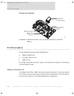
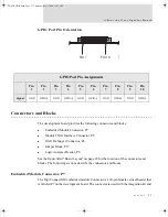
For more detailed information on connectors, switches and LEDs, see the following:
"Port Descriptions" on page 20
"Connectors and Blocks" on page 23
"Switches" on page 27
"Development Board LEDs" on page 30
"Power Jack" on page 32
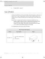
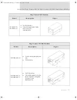
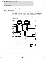
The development board accepts either of the following modules:
Module without JTAG connector—for use with an integration kit
Module with JTAG connector—for use with a development kit
See the following figures for placement of either module onto the development board.
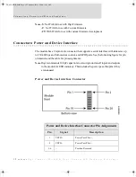
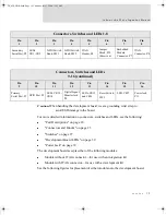
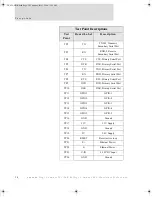
Connectors, Switches and LEDs 1-8
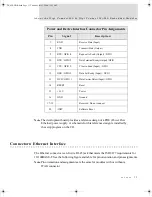
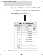
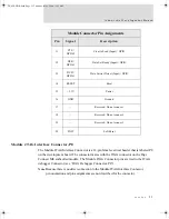
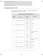
Pin
1
Pin
2
Pin
3
Pin
4
Pin
5
Pin
6
Pin
7
Pin
8
Secondary
Serial Port, P2
LEDs,
CR1 -CR9
GPIO Switch
Bank, SW1
GPIO Switch
Bank, SW2
JTAG
Header, P4
Jumper
Block, P12
(Reserved)
Embedded
Module
Connector, P7
JTAG
Connector, P8
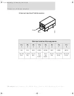
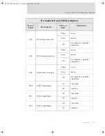
Connectors, Switches and LEDs
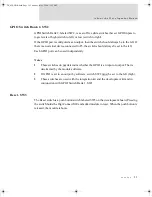
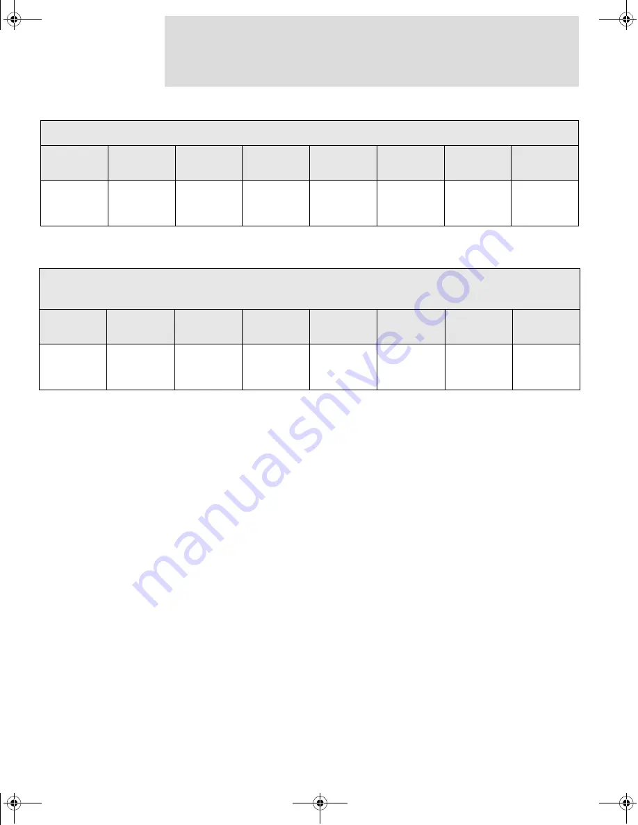
9-16 (continued)
Pin
9
Pin
10
Pin
11
Pin
12
Pin
13
Pin
14
Pin
15
Pin
16
Primary
Serial Port, P1
GPIO Port, P3
LEDs, CR10 -
CR14
Digital Signal
Monitor Jack,
P6
LEDs, CR15
and CR16
Reset Switch,
SW3
LED, CR17
Power Jack,
P11
DC_ME-HWR.book Page 19 Thursday, July 1, 2004 11:12 AM
Summary of Contents for Digi Conntect ME
Page 1: ...TM TM 90000631_A DC_ME HWR book Page 1 Thursday July 1 2004 11 12 AM...
Page 2: ...DC_ME HWR book Page 2 Thursday July 1 2004 11 12 AM...
Page 4: ...DC_ME HWR book Page 4 Thursday July 1 2004 11 12 AM...
Page 63: ...DC_ME HWR book Page 63 Thursday July 1 2004 11 12 AM...
Page 64: ...DC_ME HWR book Page 64 Thursday July 1 2004 11 12 AM...


