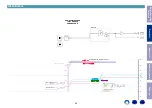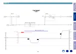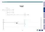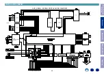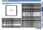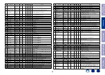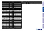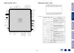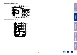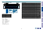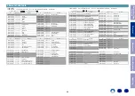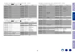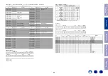
CS49844A (DIGITAL : U1073)
VDD3
BDI*, DAI1_SCLK1, GPIO71
BDI*, DAI1_D0, GPIO64
GNDIO4
VDDIO4
SD_D2, EXT_D10
SD_D11, EXT_D3
SD_D15, EXT_D7
SD_D12, EXT_D4
DAO3_D3, XMTA, GPIO113
SD_D14, EXT_D6
SD_D7, EXT_D15
SD_D13, EXT_D5
GND10
SD_D0, EXT_D8
SD_D3, EXT_D11
SD_D5, EXT_D13
SD_D1, EXT_D9
VDD9
DAO3_D7, XMTB, GPIO115
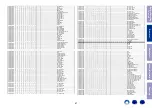
DAO3_D2, GPIO33
SCP_MOSI, GPIO147
SCP1_MISO_SDA, GPIO146
SCP1_CLK, GPIO148
SCP2_CS
SCP1_IRQ, GPIO144_OD
DAI1_SCLK2, GPIO73
VDDIO1
GNDIO1
DAI1_LRCK2, GPIO72
RESET
DBDA1
DBCK0
EE_CS0, GPIO1
DAI1_D4, GPIO68
BDI*, DAI1_D2, GPIO66
BDI*, DAI1_D1, GPIO65
SD_CS, EXT_OE
SD_BA0, EXT_A13
SD_CAS, EXT_CS2
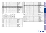
GND1
VDD2
DAI1_D5, GPIO69
EE_CS1. GPIO0
VDD10
BDI* DAI1_D3, GPIO67
VDD1
GND2
TEST_EN
SD_BA1, EXT_A14
GND3
BDI*, DAI1_LRCK1, GPIO70
SD_A10, EXT_A12
DBDA0
DBCK1
GND8
VDD8
SCP1_CS, GPIO145
SD_D4, EXT_D12
GND9
SCP_BSY, GPIO143_OD
DA03_D1, GPIO32
DA03_D5, GPIO34
DAO3_D6, GPIO35
SD_DQM0, EXT_A15
SD_WE, EXT_WE
SD_A3, EXT_A3,
SD_A2, EXT_A2
SD_D6, EXT_D14
SD_RAS, EXT_CS1
SD_A1, EXT_A1
SD_A0, EXT_A0
1
5
9
10
13
18
21
24
27
33
36
15
25
30
35
101
98
94
91
86
83
76
73
75
80
85
90
95
100
105
108
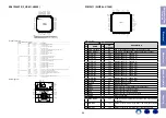
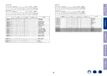
CS49844A
144-Pin LQFP
Package
(with Thermal Pad)
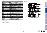
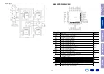
W9864G6KH-5 (DIGITAL : U1023)
Pin description
W9864G
6KH
Pub
lic
ati
on R
ele
as
e
D
ate
: N
ov
. 1
2,
2
01
3
- 4 -
Re
vis
ion
A
02
4.
PI
N C
O
NF
IG
URA
TI
O
N
54
53
52
51
50
49
48
47
46
45
44
43
42
41
40
39
38
37
36
35
34
33
32
31
30
29
28
1
2
3
4
5
6
7
8
9
10
11
12
13
14
15
16
17
18
19
20
21
22
23
24
25
26
27
DQ
0
DQ
1
DQ
2
DQ
3
DQ
4
DQ
5
DQ
6
DQ
7
LDQ
M
CA
S
RA
S
CS
BS
0
BS
1
A1
0/
AP
A0
A1
A2
A3
DQ
15
DQ
14
DQ
13
DQ
12
DQ
11
DQ
10
DQ
9
DQ
8
NC
UD
Q
M
CL
K
CK
E
NC
A1
1
A9
A8
A7
A6
A5
A4
VDD
Q
VDD
Q
VS
SQ
VS
SQ
VD
D
VD
D
VS
S
VS
SQ
VS
SQ
VDD
Q
VS
S
VS
S
W
E
VDD
VD
D
Q
W9864G6KH
Publication Release Date: Nov. 12, 2013
- 5 -
Revision A02
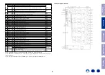
5. PIN DESCRIPTION
PIN NUMBER PIN NAME
FUNCTION
DESCRIPTION
23 ~ 26, 22,
29 ~35
A0 A11
Address
Multiplexed pins for row and column address.
Row address: A0 A11. Column address: A0 A7.
A10 is sampled during a precharge command to
determine if all banks are to be precharged or bank
selected by BS0, BS1.
20, 21
BS0, BS1
Bank Select
Select bank to activate during row address latch time,
or bank to read/write during address latch time.
2, 4, 5, 7, 8, 10,
11, 13, 42, 44,
45, 47, 48, 50,
51, 53
DQ0 DQ15
Data
Input/ Output
Multiplexed pins for data output and input.
19
CS
Chip Select
Disable or enable the command decoder. When
command decoder is disabled, new command is
ignored and previous operation continues.
18
Row Address
Strobe
Command input. When sampled at the rising edge of
the clock
,
CAS and WE define the
operation to be executed.
17
CAS
Column
Address Strobe Referred to
16
WE
Write Enable Referred to
39, 15
UDQM
LDQM
Input/output
mask
The output buffer is placed at Hi-Z (with latency of 2)
when DQM is sampled high in read cycle. In write
cycle, sampling DQM high will block the write
operation with zero latency.
38
CLK
Clock Inputs System clock used to sample inputs on the rising
edge of clock.
37
CKE
Clock Enable
CKE controls the clock activation and deactivation.
When CKE is low, Power Down mode, Suspend
mode, or Self Refresh mode is entered.
1, 14, 27
V
DD
Power
Power for input buffers and logic circuit inside DRAM.
28, 41, 54
V
SS
Ground
Ground for input buffers and logic circuit inside
DRAM.
3, 9, 43, 49
V
DDQ
Power for I/O
buffer
Separated power from V
DD
, to improve DQ noise
immunity.
6, 12, 46, 52
V
SSQ
Ground for I/O
buffer
Separated ground from V
SS
, to improve DQ noise
immunity.
36, 40
NC
No Connection No connection.
Before Servicing
This Unit
Electrical
Mechanical
Repair Information
Updating
58


