background image

AVR-2802/982

8

A/D SELECTOR

IC804

74LVX157

CODEC

D/A CONVERTER

IC801

AD1854

(2)256fs
(26)64fs
(25)fs
(27)DATA

INPUT

SELECTOR

IC505

151NS

COAXIAL

(15)

OPTICAL-1
OPTICAL-2
OPTICAL-3

(14)

(5)

(13)

OPTICAL
OUTPUT

(12)

IC506

151NS

(3)

(5)

(2)
(1)

IC800

LC89055W

CKOUT(13)

(5)DIN2

BCK

DATA

(14)

LRCK(15)

(16)

XIN

(22)

XMCK

(20)

12.288MHz

X801

MCLK

(44)

(22)

(25)

(26)

SCLKN1

LRCKN1

SDATAN1

AUDATA0 (41)

AUDATA1 (40)

AUDATA2 (39)

(30)CLKIN

IC814

CS493292

DSP

2

1

(27)

(43)

(42)

SCLK

LRCLK

CMPDAT

3

MCLK

DA SCK

DA LRCK

SD IN

256fs
64fs

fs

FRONT

SURROUND

256fs

64fs

fs

DATA

IC813

(7)

(13)

(10)

SN74LV4040APW

DIR

(6)SDTI1

IC602

AK4527

(7)SDTI2

(8)SDTI3

(39)MCLK

(4)BICK

(5)LRCK

(9)SDTO

XMT958 (3)

SURROUND BACK

CENTER/SW

SN74HC

SN74HC

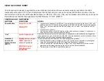
* fs is a sampling frequency of input digital signal.

e.g.:sampling frequency 48kHz fs=48kHz

* 64fs and 256fs are 64 or 256 times the sampling frequency respectively.

e.g.: sampling frequency 48kHz
64fs: 48kHz x 64=3.072MHz
256fs: 48kHz x 256=12.288MHz

* The sampling frequency for analog input is fixed to 48kHz internally.
* (No.) indicates the pin number of individual.
* The arrow indicates the direction of signal as the input terminal pointed by 

the arrow and the output terminal by the opposite.

Clock  Flow

All manuals and user guides at all-guides.com

Summary of Contents for AVR-2802

Page 1: ...g in this service manual are slightly different from the actual set For U S A Canada Europe Asia China Hong Kong Taiwan R O C model X0119 1174 NC 0112 14 14 AKASAKA 4 CHOME MINATO KU TOKYO 107 8011 JAPAN Telephone 03 3584 8111 All manuals and user guides at all guides com a l l g u i d e s c o m ...

Page 2: ...onse 5Hz 27MHz 0 3dB TUNER SECTION FM note µV at 75Ω ohms 0dBf 1 10 15 W AM Receiving Range 87 50MHz 107 90MHz 520kHz 1710kHz for U S A Canada and multiple voltage models for U S A Canada and Multiple voltage models 87 50MHz 108 00MHz 522kHz 1611kHz for Europe Asia China Hong Kong Taiwan R O C and Multiple voltage models for Europe Asia China Hong Kong Taiwan R O C and multiple voltage models Usab...

Page 3: ...form adjustment or parts replacement etc be sure to rearrange them neatly as they were originally bundled or placed afterward Otherwise incorrect arrangement can be a cause of noise generation Wire arrangement viewed from the top All manuals and user guides at all guides com ...

Page 4: ...he arrow direction 2 Front Panel 1 Remove 7 screws 3 from the top and bottom edges of the Front Panel 2 Release 4 top and bottom hooks then detach the Front Panel as shown in the arrow direction Top Cover 3 Inner Panel Pull out the Inner Panel in the arrow direction after removing 3 screws 4 Inner Panel Hook 2 2 1 3 3 3 Hook Hook Hook Front Panel 4 4 All manuals and user guides at all guides com ...

Page 5: ...Square Knob Round Knob Nut 5 Amp Connect Unit 1 Remove 3 screw to detach Pre out Unit 2 Take off the Amp Connect Unit as shown in the arrow direction after removing 1 screw 6 7 8 9 1 0 6 Regulator Unit Take off the Regulator Unit as shown in the arrow direction after removing 9 screws 1 1 6 7 8 9 1 0 1 1 All manuals and user guides at all guides com ...

Page 6: ...ar Panel 2 Take off the objective P W B upward 1 3 8 How to Check Power Control Unit with Power on 1 Remove 13 screws and 4 screws fixing to the Chassis 2 Pull up the Unit to separate from the Chassis 1 2 1 2 1 2 1 2 Rear Panel 1 4 1 3 1 3 1 3 1 3 1 3 1 3 1 4 1 4 All manuals and user guides at all guides com a l l g u i d e s c o m ...

Page 7: ... 2802 982 7 CLOCK FLOW WAVE FORM IN DIGITAL BLOCK Wave Form CH1 D DATA IC505 5 1 CH1 DATA CH2 fs CH3 64fs CH4 256fs 3 CH1 DATA CH2 DA LRCK fs CH3 DA SCK 64fs 2 All manuals and user guides at all guides com ...

Page 8: ...fs 64fs fs DATA IC813 7 13 10 SN74LV4040APW DIR 6 SDTI1 IC602 AK4527 7 SDTI2 8 SDTI3 39 MCLK 4 BICK 5 LRCK 9 SDTO XMT958 3 SURROUND BACK CENTER SW SN74HC SN74HC fs is a sampling frequency of input digital signal e g sampling frequency 48kHz fs 48kHz 64fs and 256fs are 64 or 256 times the sampling frequency respectively e g sampling frequency 48kHz 64fs 48kHz x 64 3 072MHz 256fs 48kHz x 256 12 288M...

Page 9: ...8 7 6 5 4 3 2 1 A B C D E BLOCK DIAGRAM AVR 2802 982 9 All manuals and user guides at all guides com ...

Page 10: ...8 7 6 5 4 3 2 1 A B C D E LEVEL DIAGRAMS 1 3 AVR 2802 982 10 All manuals and user guides at all guides com ...

Page 11: ...8 7 6 5 4 3 2 1 A B C D E LEVEL DIAGRAMS 2 3 AVR 2802 982 11 All manuals and user guides at all guides com a l l g u i d e s c o m ...

Page 12: ...8 7 6 5 4 3 2 1 A B C D E LEVEL DIAGRAMS 3 3 AVR 2802 982 12 All manuals and user guides at all guides com ...

Page 13: ... outlet 3 Check that the entire display is flashing with an interval of about 1 second and release your fingers from the 2 buttons and the microprocessor will be initialized Note If step 3 does not work start over from step 1 All user settings will be lost and its factory setting will be recovered when this initialization mode So make sure to memorize your setting for restoring after the initializ...

Page 14: ...Rch TP102 CENTER ch TP103 SURROUND Lch TP101 SURROUND Rch TP103 SURROUND BACK ch TP102 3 Connect power cord to AC Line and turn power switch ON 4 Presetting MASTER VOLUME counterclockwise min MODE 6CH STEREO FUNCTION CD 5 Allow 2 minutes and turn VR101 clockwise to adjust the TEST POINT voltage to 6 5 mV 0 5 mV DC 6 After 10 minutes from preset turn VR101 to set the voltage to 8 mV 0 5 mV DC 7 Adj...

Page 15: ... F MUTE O P Ed L H Front PRE OUT mute control terminal L Mute 49 P70 PRE C MUTE O P Ed L L Center PRE OUT mute control terminal L Mute 50 P71 PRE S MUTE O P Ed L L Surround PRE OUT mute control terminal L Mute 51 P72 SUB WOOFER MUTE O P Ed L H Sub woofer PRE OUT mute control terminal L Mute 52 P73 H P RELAY O P Id L H H P OUT relay control terminal L Mute 53 P74 EXP OE O P Ed L H Port expander con...

Page 16: ...O C Z L EPROM data in D6 address out A6 52 P07 AD7 AD7 I O C Z L EPROM data in D7 address out A7 53 P10 AD8 A8 A8 O C Z L EPROM address out A8 54 P11 AD9 A9 A9 O C Z L EPROM address out A9 55 P12 AD10 A10 A10 O C Z L EPROM address out A10 56 P13 AD11 A11 A11 O C Z L EPROM address out A11 57 P14 AD12 A12 A12 O C Z L EPROM address out A12 58 P15 AD13 A13 A13 O C Z L EPROM address out A13 59 P16 AD14...

Page 17: ...ontrol port data in output Parallel port type select General purpose in output 9 20 INTREQ ABOOT Control port interrupt request Automatic boot enable 21 EXTMEM GPIO8 External memory chip select General purpose in output 8 22 SDATAN1 PCM audio data input 1 25 SCLKN1 STCCLK2 PCM audio input bit clock 26 LRCLKN1 PCM audio input sample rate clock 27 CMPDAT SDATAN2 PCM audio data input 2 28 CMPCLK SCLK...

Page 18: ... Input fs cal sig out data type out input word inf output terminal 28 F2 P2 C2 O Input fs cal sig out data type out input word inf output terminal 29 VF P3 C3 O Validity flag out data type out input word inf output terminal 30 DVDD Digital power supply 31 DGND Digital GND 32 AUTO O Non PCM burst data transfer detect sig output terminal 33 BPSYNC O Non PCM burst data preamble Pa Pb Pc Pd sync sig o...

Page 19: ... output is switchable Polarity can be selected at ROM mask 15 P3 Output port P3 O General output or character background signal CO2 output is switchable Polarity can be selected at ROM mask 16 OSCOUT O Terminal for external use of sync signal OSC circuit Use the freq 14 32MHz at NTSC 17 OSCIN I system 17 73MHz at PAL system 14 30MHz at MPAL system 18 HOR Horizontal sync signal I Inputs horizontal ...

Page 20: ...NC No Connect No internal bonding 20 ADIF I Analog Input Format Select pin 21 CAD1 I Chip address 1 pin 22 CAD0 I Chip address 0 pin 23 LOUT3 O DAC3L channel analog out pin 24 ROUT3 O DAC3R channel analog out pin 25 LOUT2 O DAC2L channel analog out pin 26 ROUT2 O DAC2R channel analog out pin 27 LOUT1 O DAC1L channel analog out pin 28 ROUT1 O DAC1R channel analog out pin 29 LIN I L ch analog invert...

Page 21: ...8 AM 29 AM 30 AM 31 AM 32 G7 G8 G9 G10 G11 AA8 G12 AA7 G13 AA6 G14 AA5 G15 AA4 G16 AA3 AA2 AA1 AM35 AM34 AM33 DI CL CE RES VDD OSCI OSCO Vss TEST VFL G1 G2 G3 G4 G5 G6 Symbol VDD Vss Power terminal 5V Power terminal GND VFL Power terminal FL drive DI CL CE Serial data transfer terminal DI Data CL Clock CE Chip enable OSCI OSCO External CR connecting terminal RES System reset terminal AM1 AM35 AA1 ...

Page 22: ...ction Terminal Function No 1 DGND I Digital Ground 2 MCLK I Master Clock Input 3 CLATCH I Latch input for control data 4 CCLK I Control clock input for control data 5 CDATA I Serial control input 6 384 256 I Selects the master clock mode 7 X2MCLK I Selects internal clock doubler LO or internal clock MCLK HI 8 ZEROR O Right Channel Zero Flag Output 9 DEEMP I De Emphasis 10 96 48 I Selects 48kHz LO ...

Page 23: ...el shift circuit TC9459N EX IC805 1 2 3 4 5 6 7 8 9 10 11 12 13 14 28 27 26 25 24 23 22 21 20 19 18 17 16 15 Vss NC L OUT NC L IN L LD1 L LD2 L A GND NC CS1 GND CK V NC R OUT NC R IN R LD1 R LD2 R A GND NC CS2 DATA NC STB NC NC DD 1 2 3 4 5 6 7 8 9 10 11 12 13 14 28 27 26 25 24 23 22 21 20 19 18 17 16 15 Vss NC L OUTA L A GNDB CS1 GND CK V TEST R OUTA R A GNDB DATA L A GNDC STB DD L INC L OUTC L I...

Page 24: ...4 13 12 11 10 9 5 D2 D1 D0 Y W S D4 D5 D6 D7 A B C 3 2 1 0 Y W Strobe GND Vcc 4 5 6 7 A B C Data Inputs Data Select Data Inputs Outputs BU4051BCF AU IC251 252 504 507 Channel IN OUT X4 X6 X X7 X5 INHIBIT VEE Vss VDD X2 X1 X0 X3 A B C Common Channel IN OUT OUT IN 1 2 3 4 5 6 7 8 16 15 14 13 12 11 10 9 4 C 6 OUT IN 7 5 INH VEE 2 1 0 3 A B TC74VHC123AF AU IC801 15 1 2 3 4 5 6 7 8 5 16 14 13 12 11 10 ...

Page 25: ...ysteresis Comparator FRONT VIEW Input GND Output FRONT VIEW Vcc GND Vout GP1FA551RZ EX IC501 503 VCC VOUT GND Vin Vcc GND GP1FA551TZ EX IC707 VCC Vin GND INPUT DRIVE IC OPTICAL OUTPUT FRONT VIEW A OUTPUT A INPUT A INPUT V B OUTPUT V B INPUT B INPUT 1 2 3 4 5 7 8 6 1 2 TOP VIEW Vout Vcc GND LC72720NM CO IC105 Europe Model Only TOP VIEW IN OUT GND 1 2 3 4 5 6 7 8 9 10 11 12 V MPXIN FLOUT CIN T1 T2 T...

Page 26: ...4EK DTC114EK DTC114ES DTC143EK DTC144EK DTC323TK MP15P MN15N ESCDB B D C E S R 70W Typ RE 0 22W Typ BDCSE B D C E S R 70W Typ RE 0 22W Typ DIODES included LED 1SR35 400A 1SS270A RB721Q 40 2 3 1 HZS3C 2 HZS5C 1 HZS6A 1 HZS6A 2 HZS7B 2 HZS9B 1 HZS33 2 MTZJ18A S4VB20 S4VB20F SEL1210S Red SEL1410E Green DAN202K 1 Anode 2 Anode 3 Cathode FRONT VIEW B C E FRONT VIEW B C E TOP VIEW D S G FRONT VIEW B C E...

Page 27: ... 1 VDP TAPE DVD MD AUX DVD MD V AUX TUNER 2 3 CD 1 PHONO VCR REC MULTI STEREO AUTO TUNED RDS CH S1 S2 S3 S4 S5 S6 S7 S8 S9 S10 S11 S12 S1 S2 S3 S4 S5 S6 S7 S9 S10 S11 S12 S1 S2 S3 S4 S5 S6 S7 S8 S9 S10 S11 S12 S13 S14 S15 S16 S17 S18 S19 S20 S21 S22 S23 S24 S13 S14 S15 S25 S26 S27 S28 S29 S30 S31 S32 S33 S34 S35 S25 S26 S27 S28 S29 S30 S31 S32 S33 S34 S35 G2 G16 G1 G2 G16 G1 G2 G16 G1 G2 G16 G1 DI...

Page 28: ... 1 7 1 9 1 5 1 5 1 5 1 5 1 5 1 10 1 2 1 2 1 2 1 2 1 3 1 3 7 1 4 8 7 6 5 4 3 2 1 A B C D E PRINTED WIRING BOARDS AVR 2802 982 28 COMPONENT SIDE 1U 3368 POWER P W B Ass y All manuals and user guides at all guides com ...

Page 29: ... 1 11 1 10 1 9 1 10 1 12 1 15 1 12 1 4 1 8 16 9 15 28 14 1 15 28 14 1 42 22 1 21 8 7 6 5 4 3 2 1 A B C D E AVR 2802 982 29 COMPONENT SIDE 1U 3369 EXT IN P W B Ass y All manuals and user guides at all guides com ...

Page 30: ...B E C B E C B E C B E C B E C B E 1 8 9 16 1 4 5 8 1 4 5 8 1 4 5 8 1 4 5 8 1 4 5 8 1 4 5 8 1 4 5 8 1 4 5 8 1 4 5 8 1 4 5 8 1 4 5 8 1 4 5 8 1 8 9 16 1 7 8 14 8 7 6 5 4 3 2 1 A B C D E AVR 2802 982 30 FOIL SIDE 1U 3369 EXT IN P W B Ass y All manuals and user guides at all guides com ...

Page 31: ...9 1 9 1 1 1 19 11 2 2 2 18 10 14 13 1 2 14 13 1 13 2 12 1 8 1 8 1 11 1 11 1 10 1 12 1 15 1 15 1 15 8 7 6 5 4 3 2 1 A B C D E AVR 2802 982 31 COMPONENT SIDE 1U 3370 CONTROL P W B Ass y All manuals and user guides at all guides com a l l g u i d e s c o m ...

Page 32: ...E C B E C B E C B E C B E C B E C B E C B E C B E C B E C B E 1 16 17 32 33 48 62 1 8 9 16 1 8 9 16 1 8 9 16 1 13 12 49 50 51 75 76 100 24 1 25 26 8 7 6 5 4 3 2 1 A B C D E AVR 2802 982 32 FOIL SIDE 1U 3370 CONTROL P W B Ass y All manuals and user guides at all guides com ...

Page 33: ... 5 1 1 3 2 1 5 1 5 1 5 1 5 1 1 11 19 2 2 10 1 11 2 10 18 1 3 1 2 1 15 1 15 1 1 1 2 14 15 12 4 3 8 7 6 5 4 3 2 1 A B C D E AVR 2802 982 33 COMPONENT SIDE 1U 3371 AMP CONNECT P W B Ass y All manuals and user guides at all guides com ...

Page 34: ...C B E C B E C B E C B E C B E C B E C B E C B E C B E C B E C B E C B E C B E C B E C B E C B E 8 7 6 5 4 3 2 1 A B C D E AVR 2802 982 34 FOIL SIDE 1U 3371 AMP CONNECT P W B Ass y All manuals and user guides at all guides com ...

Page 35: ... 1 9 8 16 1 9 8 16 1 9 8 16 1 9 8 16 1 9 8 16 1 9 8 16 1 9 8 16 1 9 8 16 1 1 9 8 10 11 20 1 9 10 18 16 1 1 9 8 4 5 8 1 4 5 8 1 4 5 8 1 4 5 8 1 4 5 8 1 4 5 8 1 4 5 8 1 4 5 8 16 1 7 8 14 1 8 9 16 1 8 9 16 1 8 9 16 1 4 5 8 1 4 5 8 1 4 5 8 15 28 1 14 22 42 1 21 1 14 15 28 1 25 26 50 51 100 101 125 1 11 12 22 23 33 34 44 1 5 4 13 14 20 21 29 30 8 7 6 5 4 3 2 1 A B C D E AVR 2802 982 35 COMPONENT SIDE 1...

Page 36: ...C B E C B E C B E C B E C B E C B E 1 4 5 8 1 4 5 8 1 4 5 8 1 4 5 8 1 10 11 20 1 4 5 8 8 7 6 5 4 3 2 1 A B C D E AVR 2802 982 36 FOIL SIDE 1U 3373 AUDIO DSP P W B Ass y All manuals and user guides at all guides com a l l g u i d e s c o m ...

Page 37: ...nd possibly to take a long period of time for supplying or in some case supplying of part may be refused l When ordering of part clearly indicate 1 and I i to avoid mis supplying l Ordering part without stating its part number can not be supplied l Part indicated with the mark is not illustrated in the exploded view l Not including Carbon Film 5 1 4W Type in the P W Board parts list Refer to the S...

Page 38: ...m 1 kohm 1 4W NB RD14B2E102JNBST R219 220 241 2379 987 Carbon film 1 kohm 1 4W NB RD14B2E102JNBST R223 224 241 2378 920 Carbon film 220 ohm 1 4W NB RD14B2E221JNBST R225 226 244 2671 914 Metal oxide 15 kohm 2W NB RS14B3D153JNBST S R227 228 241 2378 946 Carbon film 270 ohm 1 4W NB RD14B2E271JNBST SEMICONDUCTORS GROUP IC501 263 1100 018 IC KIA7806API IC502 268 0073 905 IC ICP N15 TR101 102 273 0459 9...

Page 39: ... 926 Semi fixed resistor 220 ohm V06PB221T VR201 202 211 6131 926 Semi fixed resistor 220 ohm V06PB221T VR301 211 6131 926 Semi fixed resistor 220 ohm V06PB221T VR401 211 6131 926 Semi fixed resistor 220 ohm V06PB221T CAPACITORS GROUP C101 102 254 4538 939 Electrolytic 47 uF 16V CE04W1C470MT SMG RE3 For EU 982 EC E1 E1H E1C EUT 254 4538 942 Electrolytic 100 uF 16V CE04W1C101MT SMG RE3 For E2 C103 ...

Page 40: ... 220 pF 50V CK45B1H221KT DD 3 C409 255 1264 908 Mylar film 1000 pF 50V CQ93M1H102JT B C411 253 4482 901 Ceramic 33 pF 500V CC45SL2H330JT C413 254 4538 942 Electrolytic 100 uF 16V CE04W1C101MT SMG RE3 C415 253 4486 907 Ceramic 47 pF 500V CC45SL2H470JT C417 253 4465 902 Ceramic 5 pF 500V CC45SL2H050CT C419 255 1275 942 Mylar film 220 pF 100V CQ93M2A221KT B C421 254 4527 982 Electrolytic 10 uF 100V C...

Page 41: ...MD IC312 262 2919 001 IC TC9274N 017 IC501 503 269 0194 007 Optical connector GP1FA551RZ IC504 262 1205 907 IC TC74HCU04AF IC505 506 262 2386 906 IC SN74HC151NS IC701 263 0896 909 IC NJM2068MD IC707 269 0187 001 Optical connector GP1FA551TZ IC801 263 0896 909 IC NJM2068MD For EU 982 EC 263 0898 907 IC NJM5532MD For E2 E1 E1H E1C EUT IC802 804 263 0896 909 IC NJM2068MD IC805 262 2662 002 IC TC9459N...

Page 42: ...1JT For E2 E1 E1H E1C EUT R403 404 247 2015 964 Carbon chip 2 7 Mohm 1 16W RM73B 275KT R417 418 247 2005 903 Carbon chip 100 ohm 1 16W RM73B 101JT For EU 982 EC 247 2006 960 Carbon chip 470 ohm 1 16W RM73B 471JT For E2 E1 E1H E1C EUT R419 420 247 2015 964 Carbon chip 2 7 Mohm 1 16W RM73B 275KT R433 438 247 2011 926 Carbon chip 39 kohm 1 16W RM73B 393JT R439 440 247 2004 920 Carbon chip 47 ohm 1 16...

Page 43: ... 104JT R857 247 2009 983 Carbon chip 10 kohm 1 16W RM73B 103JT R858 247 2007 943 Carbon chip 1 kohm 1 16W RM73B 102JT R859 860 247 2011 942 Carbon chip 47 kohm 1 16W RM73B 473JT R867 869 247 2011 942 Carbon chip 47 kohm 1 16W RM73B 473JT R871 872 247 2011 942 Carbon chip 47 kohm 1 16W RM73B 473JT R874 875 247 2011 942 Carbon chip 47 kohm 1 16W RM73B 473JT R883 888 247 2012 925 Carbon chip 100 kohm...

Page 44: ... 998 Electrolytic 22 uF 50V CE04W1H220MT SMG RE3 CAPACITORS GROUP C101 102 254 4524 956 Electrolytic 2 2 uF 50V CE04W1H2R2MT SMG RE3 C105 106 254 4524 969 Electrolytic 3 3 uF 50V CE04W1H3R3MT SMG RE3 C107 108 256 1058 942 Metalized 0 056 uF 50V CF93A1H563JT JL C109 110 255 1265 907 Mylar film 6800 pF 50V CQ93M1H682JT B C111 112 257 0506 951 Ceramic chip 100 pF 50V CC73CH1H101JT C113 114 255 1265 9...

Page 45: ... Inductor 2 2uH 1 L504 505 235 0060 918 Inductor 4 7uH 2 L701 702 235 9003 002 FTZ choke coil For E2 EUT 2 RL901 214 0203 008 Relay NA12W K 1 W708 709 205 1034 010 M3 Screw terminal 2 W726 203 0525 003 1P SIN cord Ass y 1 W731 203 0463 000 1P SIN con Ass y 1 1U 3370 CONTROL UNIT ASS Y SEMICONDUCTORS GROUP IC101 262 2549 002 IC LC75721E IC102 499 0290 007 Remote sensor GP1U271X IC103 262 2745 903 I...

Page 46: ...34 247 2009 983 Carbon chip 10 kohm 1 16W RM73B 103JT R335 247 2011 942 Carbon chip 47 kohm 1 16W RM73B 473JT R340 247 2009 909 Carbon chip 4 7 kohm 1 16W RM73B 472JT 1608 R341 342 247 2009 983 Carbon chip 10 kohm 1 16W RM73B 103JT R343 344 247 2005 903 Carbon chip 100 ohm 1 16W RM73B 101JT R345 247 2018 903 Carbon chip 0 ohm 1 16W RM73B 0R0KT R346 247 2005 903 Carbon chip 100 ohm 1 16W RM73B 101J...

Page 47: ... Electrolytic 220 uF 6 3V CE04W0J221MT SMG RE3 C376 257 0509 929 Ceramic chip 1000 pF 50V CK73B1H102KT C377 254 4538 900 Electrolytic 10 uF 16V CE04W1C100MT SMG RE3 C378 257 0509 929 Ceramic chip 1000 pF 50V CK73B1H102KT For EU 982 EC E2 C380 257 0516 909 Ceramic chip 0 022 uF 25V CK73B1E223KT C390 256 1058 971 Metalized 0 1 uF 50V CF93A1H104JT JL C392 257 0509 929 Ceramic chip 1000 pF 50V CK73B1H...

Page 48: ...nsistor 2SC3311A TR901 273 0429 904 Transistor 2SC3311A TR904 272 0158 007 Transistor 2SB KTB778 R O TR918 272 0158 007 Transistor 2SB KTB778 R O D903 904 276 0432 903 Diode 1SS270A D913 915 276 0305 001 Diode S4VB20 D918 919 276 0432 903 Diode 1SS270A PT901 279 0034 054 Posistor PTH9M04BC222TS2F333 RESISTORS GROUP R501 504 247 2006 960 Carbon chip 470 ohm 1 16W RM73B 471JT For EU 982 EC 247 2006 ...

Page 49: ... 0R0KT R910 241 2376 919 Carbon film 30 ohm 1 4W NB RD14B2E300JNBST R949 241 2376 919 Carbon film 30 ohm 1 4W NB RD14B2E300JNBST CAPACITORS GROUP C501 504 254 4538 913 Electrolytic 22 uF 16V CE04W1C220MT SMG RE3 For EU 982 EC 254 4538 942 Electrolytic 100 uF 16V CE04W1C101MT SMG RE3 For E2 E1 E1H E1C EUT C507 254 4524 943 Electrolytic 1 uF 50V CE04W1H010MT SMG RE3 C511 254 4538 913 Electrolytic 22...

Page 50: ...C 5 SEMICONDUCTORS GROUP IC107 262 2545 006 IC TC9274N 011 IC108 262 2033 000 IC TC9273N 004 IC109 263 0896 909 IC NJM2068MD IC112 263 0615 902 IC BA15218F IC251 252 262 2826 903 IC BU4051BCF IC253 254 263 1082 903 IC TK15420MTL IC255 262 2012 908 IC BU4052BCFT1 IC256 262 2013 907 IC BU4053BCFT1 IC257 263 1082 903 IC TK15420MTL IC301 262 2983 105 IC TMP93CS40F IC451 262 2827 902 IC MM74HC4053SJ IC...

Page 51: ...JT R304 247 2009 909 Carbon chip 4 7 kohm 1 16W RM73B 472JT 1608 R305 306 247 2003 989 Carbon chip 33 ohm 1 16W RM73B 330JT R307 247 2009 983 Carbon chip 10 kohm 1 16W RM73B 103JT R308 247 2003 989 Carbon chip 33 ohm 1 16W RM73B 330JT R309 247 2009 983 Carbon chip 10 kohm 1 16W RM73B 103JT R311 312 247 2003 989 Carbon chip 33 ohm 1 16W RM73B 330JT R313 247 2009 983 Carbon chip 10 kohm 1 16W RM73B ...

Page 52: ...5 546 247 2008 913 Carbon chip 2 kohm 1 16W RM73B 202JT R549 550 247 2009 983 Carbon chip 10 kohm 1 16W RM73B 103JT R551 554 247 2005 903 Carbon chip 100 ohm 1 16W RM73B 101JT R555 556 247 2009 983 Carbon chip 10 kohm 1 16W RM73B 103JT R557 247 2006 973 Carbon chip 510 ohm 1 16W RM73B 511JT R558 247 2006 960 Carbon chip 470 ohm 1 16W RM73B 471JT R559 247 2006 999 Carbon chip 620 ohm 1 16W RM73B 62...

Page 53: ...hip 1 kohm 1 16W RM73B 102JT R898 247 2005 903 Carbon chip 100 ohm 1 16W RM73B 101JT R924 247 2009 909 Carbon chip 4 7 kohm 1 16W RM73B 472JT 1608 R925 948 247 2005 903 Carbon chip 100 ohm 1 16W RM73B 101JT R949 247 2018 903 Carbon chip 0 ohm 1 16W RM73B 0R0KT R951 247 2018 903 Carbon chip 0 ohm 1 16W RM73B 0R0KT R955 957 247 2004 920 Carbon chip 47 ohm 1 16W RM73B 470JT R961 962 247 2004 920 Carb...

Page 54: ...4 4524 985 Electrolytic 10 uF 50V CE04W1H100MT SMG RE3 C622 257 0506 951 Ceramic chip 100 pF 50V CC73CH1H101JT C623 257 0512 903 Ceramic chip 0 1 uF 25V CK73F1E104ZT C624 254 4536 928 Electrolytic 100 uF 10V CE04W1A101MT SMG RE3 C625 254 4524 956 Electrolytic 2 2 uF 50V CE04W1H2R2MT SMG RE3 C626 257 0512 903 Ceramic chip 0 1 uF 25V CK73F1E104ZT C627 254 4538 900 Electrolytic 10 uF 16V CE04W1C100MT...

Page 55: ...mic chip 0 01 uF 50V CK73F1H103ZT C938 257 0512 903 Ceramic chip 0 1 uF 25V CK73F1E104ZT C939 257 0511 904 Ceramic chip 0 01 uF 50V CK73F1H103ZT OTHER PARTS GROUP CW061 205 0942 019 6P connector socket TUC P 1 CW072 205 0942 022 7P connector socket TUC P 1 CW081 082 205 0885 095 8P connector socket TUC P 2 CW086 205 0885 095 8P connector socket TUC P 1 CW093 205 0885 037 9P connector socket TUC P ...

Page 56: ... E1 E1H model E2 E1 E1C E1H EUT model 4 4 EU EC model 24 5 2 19 102 104 27 27 104 109 104 109 104 111 112 36 1 3 112 111 36 5 4 7 4 5 8 7 6 5 4 3 2 1 A B C D E EXPLODED VIEW AVR 2802 982 56 WARNING Parts marked with this symbol have critical characteristics Use ONLY replacement parts recommended by the manufacturer The symbols indicate the following distinations EU U S A model EC Canada model E2 E...

Page 57: ... W 12 107 473 7004 016 4X6 CBTS S Z 4 108 473 8064 000 4X8 CBTS B B 3P For Black model 6 473 8064 013 4X8 CBTS B N 3P For Gold model 6 109 477 0064 107 Fixing screw For EU 982 EC EUT E1 E1H 36 For E2 E1C 34 110 473 8034 098 3X10 CBTS B B 4 111 473 7500 028 3X8 CFTS P Z 6 112 473 7002 034 3X6 CBTS S B 2 113 473 8034 056 3X14 CBTS B Z 7 114 473 7002 005 3X6 CBTS S Z 6 PARTS LIST OF EXPLODED VIEW Ref...

Page 58: ...M ANT ass y for E2 1 208 529 0079 008 FM ANT adapter for E1 E1C E1H EUT 1 209 399 0757 004 Remote controller RC 903 for EU EC E1 E1C E1H EUT 1 209 399 0757 017 Remote controller RC 904 for E2 1 210 515 0867 101 S S list EX 1 211 501 2100 087 Carton case for EU EC E2 E1 E1C EUT 1 211 501 2100 090 Carton case for EU AVR 982 1 211 501 2099 033 Carton case for E1H 1 212 Control card 1 214 515 0817 009...

Page 59: ...8 7 6 5 4 3 2 1 A B C D E WIRING DIAGRAM AVR 2802 982 59 All manuals and user guides at all guides com ...

Page 60: ...UT PRIOR NOTICE Parts marked with this symbol have critical characteristics Use ONLY replacement parts recommended by the manufacture CAUTION Before returning the unit to the customer make sure you make either 1 a leakage current check or 2 a line to chassis resistance check If the leakage current exceeds 0 5 milliamps or if the resistance from chassis to either side of the power card is less than...

Page 61: ...RIOR NOTICE Parts marked with this symbol have critical characteristics Use ONLY replacement parts recommended by the manufacture CAUTION Before returning the unit to the customer make sure you make either 1 a leakage current check or 2 a line to chassis resistance check If the leakage current exceeds 0 5 milliamps or if the resistance from chassis to either side of the power card is less than 460...

Page 62: ...SCHEMATIC DIAGRAMS 1 12 1 2 3 4 5 6 All manuals and user guides at all guides com ...

Page 63: ... 12V AVR 2802 982 6 7 8 9 10 11 A B C D All manuals and user guides at all guides com ...

Page 64: ...NOTICE NOTICE ALL RESISTANCE VALU ALL CAPACITANCE VA EACH VOLTAGE AND C CONDITION CIRCUIT AND PARTS A NOTICE All manuals and user guides at all guides com ...

Page 65: ...ics Use ONLY replacement parts recommended by the manufacture CAUTION Before returning the unit to the customer make sure you make either 1 a leakage current check or 2 a line to chassis resistance check If the leakage current exceeds 0 5 milliamps or if the resistance from chassis to either side of the power card is less than 460kohms the unit is defective WARNING DO NOT return the unit to the cu...

Page 66: ... WARNING Parts marked with this symbol have critical characteristics Use ONLY replacement parts recommended by the manufacture CAUTION Before returning the unit to the customer make sure you make either 1 a leakage current check or 2 a line to chassis resistance check If the leakage current exceeds 0 5 milliamps or if the resistance from chassis to either side of the power card is less than 460koh...

Page 67: ...WITHOUT PRIOR NOTICE WARNING Parts marked with this symbol have critical characteristics Use ONLY replacement parts recommended by the manufacture CAUTION Before returning the unit to the customer make sure you make either 1 a leakage current check or 2 a line to chassis resistance check If the leakage current exceeds 0 5 milliamps or if the resistance from chassis to either side of the power card...

Page 68: ... 2 5V SCHEMATIC DIAGRAMS 2 12 1 2 3 4 5 6 All manuals and user guides at all guides com ...

Page 69: ... 5V 5V 5V AVR 2802 982 6 7 8 9 10 11 A B C D All manuals and user guides at all guides com ...

Page 70: ... 3 3V 2 5V NOTICE ALL RESISTANCE VAL ALL CAPACITANCE VA EACH VOLTAGE AND C CONDITION CIRCUIT AND PARTS A NOTICE All manuals and user guides at all guides com ...

Page 71: ... replacement parts recommended by the manufacture CAUTION Before returning the unit to the customer make sure you make either 1 a leakage current check or 2 a line to chassis resistance check If the leakage current exceeds 0 5 milliamps or if the resistance from chassis to either side of the power card is less than 460kohms the unit is defective WARNING DO NOT return the unit to the customer until...

Page 72: ...ARE SUBJECT TO CHANGE WITHOUT PRIOR NOTICE WARNING Parts marked with this symbol have critical characteristics Use ONLY replacement parts recommended by the manufacture CAUTION Before returning the unit to the customer make sure you make either 1 a leakage current check or 2 a line to chassis resistance check If the leakage current exceeds 0 5 milliamps or if the resistance from chassis to either ...

Page 73: ...D PARTS ARE SUBJECT TO CHANGE WITHOUT PRIOR NOTICE WARNING Parts marked with this symbol have critical characteristics Use ONLY replacement parts recommended by the manufacture CAUTION Before returning the unit to the customer make sure you make either 1 a leakage current check or 2 a line to chassis resistance check If the leakage current exceeds 0 5 milliamps or if the resistance from chassis to...

Page 74: ...All manuals and user guides at all guides com ...

Reviews: