Chapter 2
10
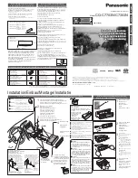
To aid the discussions in this chapter, refer to the block diagram of a
DT3130 Series board, shown in
. Bold signal names indicate
signals you can access.
Figure 1: DT3130 Series Block Diagram
Secondary PCI Bus
Primary PCI Bus
PCI to PCI
Bridge
PCI Interface
Counter/Strobe
Function Block
Sync Stripper
Hsync
Vs
ync
Hsync
Hsync
Vs
ync
Vs
ync
Isolation (on -ISO
models only)
Trigger Inputs [0:2]*
Video Inputs
[0:2]*
Video Inputs
[3:5]*
Video Inputs
[6:8]*
Trigger 0
ADC 0
ADC 1
ADC 2
Trigger 1
Trigger 2
Strobe Outputs [0:2*]
**Video inputs 3 to 5, Trigger Input 1, and Strobe Output 1 are
supported on the DT3132, DT3132-ISO, DT3133, and DT3133-ISO
boards only. Video inputs 6 to 8, Trigger Input 2, and Strobe
Output 2 are supported on the DT3133 and DT3133-ISO boards
12 VDC Aux. Power
Clock
Synchronization
Acquire Clock
(28.6 MHz)
MUX0
MUX2
MUX1
Programmable
Image Scaling
Programmable
Image Cropping
FIFO
0
0
1
1
2
2
Summary of Contents for DT3130 Series
Page 1: ...DT3130 Series UM 17314 G User s Manual ...
Page 4: ......
Page 8: ...Contents viii ...
Page 16: ...About this Manual xvi ...
Page 17: ...1 1 Overview Features 2 Supported Software 5 Accessories 7 ...
Page 24: ...Chapter 1 8 ...
Page 56: ...Chapter 2 40 ...
Page 119: ...103 A Specifications ...
Page 126: ...Appendix A 110 ...
Page 134: ...Appendix B 118 ...
Page 154: ...Index 138 ...
Page 156: ......
Page 160: ......