


DS21354 & DS21554
11 of 117
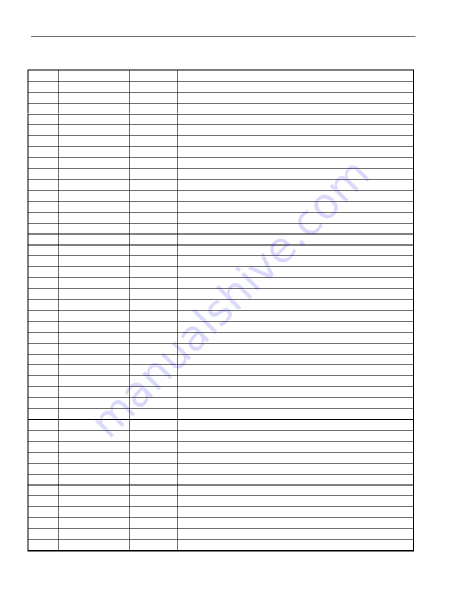
4 PIN DESCRIPTION
PIN DESCRIPTION SORTED BY PIN NUMBER
Table 4-1
PIN
SYMBOL
TYPE
DESCRIPTION
1
RCHBLK
O
Receive Channel Block
2
JTMS
I
IEEE 1149.1 Test Mode Select
3
8MCLK
O
8.192 MHz Clock
4
JTCLK
I
IEEE 1149.1 Test Clock Signal
5
JTRST*
I
IEEE 1149.1 Test Reset
6
RCL
O
Receive Carrier Loss
7
JTDI
I
IEEE 1149.1 Test Data Input
8
NC
–
No Connect (do not connect any signal to this pin)
9
NC
–
No Connect (do not connect any signal to this pin)
10
JTDO
O
IEEE 1149.1 Test Data Output
11
BTS
I
Bus Type Select
12
LIUC
I
Line Interface Connect
13
8XCLK
O
Eight Times Clock
14
TEST
I
Test
15
NC
–
No Connect (do not connect any signal to this pin)
16
RTIP
I
Receive Analog Tip Input
17
RRING
I
Receive Analog Ring Input
18
RVDD
–
Receive Analog Positive Supply
19
RVSS
–
Receive Analog Signal Ground
20
RVSS
–
Receive Analog Signal Ground
21
MCLK
I
Master Clock Input
22
XTALD
O
Quartz Crystal Driver
23
NC
–
No Connect
24
RVSS
–
Receive Analog Signal Ground
25
INT*
O
Interrupt
26
NC
–
No Connect (do not connect any signal to this pin)
27
NC
–
No Connect (do not connect any signal to this pin)
28
NC
–
No Connect (do not connect any signal to this pin)
29
TTIP
O
Transmit Analog Tip Output
30
TVSS
–
Transmit Analog Signal Ground
31
TVDD
–
Transmit Analog Positive Supply
32
TRING
O
Transmit Analog Ring Output
33
TCHBLK
O
Transmit Channel Block
34
TLCLK
O
Transmit Link Clock
35
TLINK
I
Transmit Link Data
36
CI
I
Carry In
37
TSYNC
I/O
Transmit Sync
38
TPOSI
I
Transmit Positive Data Input
39
TNEGI
I
Transmit Negative Data Input
40
TCLKI
I
Transmit Clock Input
41
TCLKO
O
Transmit Clock Output
42
TNEGO
O
Transmit Negative Data Output
43
TPOSO
O
Transmit Positive Data Output


