38
FX3 Programmers Manual, Doc. # 001-64707 Rev. *C
FX3 Overview
Certain pins, like the USB lines have specific electrical characteristics and are connected directly to
the USB IO-System. They do not have GPIO capability.
Pins belonging to the same block share the same group setting (say alpha) for drive strengths. Pins
of a block overridden as GPIO share the same group setting (say beta) for their drive strength. FX3
provides software controlled pull up (50 k
Ώ
) or pull down (10 k
Ώ
) resistors internally on all digital I/O
pins.
3.6.6
GPIF
The FX3 device includes a GPIF II interface that provides an easy and glue less interface to popular
interfaces such as asynchronous SRAM, synchronous SRAM, Address Data Multiplexed interface,
parallel ATA, and so on. The interface supports up to 100 MHz. and has 40 programmable pins that
are programmed by GPIF Waveform Descriptor as data, address, control, or GPIO function. For
example, the GPIF II can be configured to a 16-bit ADM (Address/Data Multiplex), seven control
signals, and seven GPIO
The GPIF II interface features the following:
■
The ability to play both the master and slave role, eliminating the need for a separate slave FIFO
interface.
■
A large state space (256 states) to enable more complex pipelined signaling protocols.
■
A wider data path supporting 32-bit mode in addition to 16- and 8-bit.
■
A deeper pipeline designed for substantially higher speed (more than 200 MHz internal clock
frequency - “Edge Placement Frequency")
■
High frequency I/Os with DLL timing correction (shared with other interface modes), enabling
interface frequencies of up to 100 MHz.
■
40 programmable pins
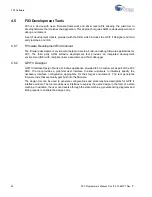
The heart of the GPIF II interface is a programmable state machine.
Figure 3-10. State Machine
This state machine
■
Supports up to 256 different states
■
Monitors up to 32 input signals (lamda) to transition between states
■
Provides for transition to two different states from the current state
■
Can drive/control up to eight external pins of the device (omega)
■
Can generate up to 33 different internal control signals (sigma)
The GPIF II is not connected directly to the USB endpoint buffers. Instead it is connected to FX3's
internal DMA network. This enables the FX3's high-performance CPU to have more control over and
access to the data flows in the application thus enabling a wider range of applications, including
ones that process, rather than just route, the actual data flows.
GPIF II
STATE
MACH.
(256 states)
λ
ω
σ
Lamda
(32)
Omega
(8)
Sigma
(33)
Summary of Contents for EX-USB FX3
Page 8: ...8 FX3 Programmers Manual Doc 001 64707 Rev C Contents...
Page 12: ...12 FX3 Programmers Manual Doc 001 64707 Rev C Introduction...
Page 48: ...48 FX3 Programmers Manual Doc 001 64707 Rev C FX3 Overview...
Page 74: ...74 FX3 Programmers Manual Doc 001 64707 Rev C FX3 Firmware...
Page 76: ...76 FX3 Programmers Manual Doc 001 64707 Rev C FX3 APIs...
Page 84: ...84 FX3 Programmers Manual Doc 001 64707 Rev C FX3 Application Examples...
Page 98: ...98 FX3 Programmers Manual Doc 001 64707 Rev C FX3 Application Structure...
Page 148: ...148 FX3 Programmers Manual Doc 001 64707 Rev C FX3 P Port Register Access...
Page 165: ...FX3 Programmers Manual Doc 001 64707 Rev C 165 FX3 Development Tools Click next...
Page 178: ...178 FX3 Programmers Manual Doc 001 64707 Rev C FX3 Development Tools Click on Apply...
Page 180: ...180 FX3 Programmers Manual Doc 001 64707 Rev C FX3 Development Tools d Start the GDB server...
Page 185: ...FX3 Programmers Manual Doc 001 64707 Rev C 185 FX3 Development Tools...
Page 186: ...186 FX3 Programmers Manual Doc 001 64707 Rev C FX3 Development Tools...
Page 187: ...FX3 Programmers Manual Doc 001 64707 Rev C 187 FX3 Development Tools...
Page 188: ...188 FX3 Programmers Manual Doc 001 64707 Rev C FX3 Development Tools...
Page 192: ...192 FX3 Programmers Manual Doc 001 64707 Rev C GPIF II Designer...


