background image

4. Functions 


48


ADA16-32/2(PCI)F 

Stop Condition 

The condition for controlling the stop of sampling can be selected from among the last sampling count, 

input data comparison, an external trigger, and software abort. 

The board stops sampling whenever an error occurs irrespective of the stop condition setting. 

Last sampling count 

The board stops sampling after storing input data to memory for the specified number of times of 

sampling. 

- Input 

data 

comparison 

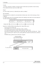
Once the board has started sampling, it compares the analog signal input through a specified 

channel to the value of the preset comparison level.    If the analog signal satisfies the condition, the 

board stops sampling. 

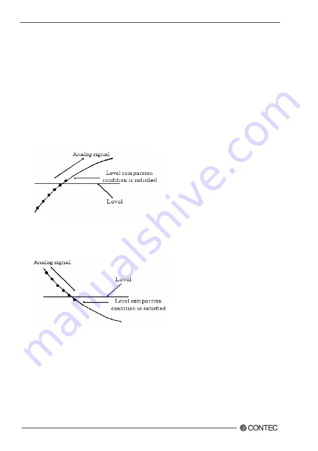
Level comparison conditions are set as two conditions: level and direction. 


The above sketch shows that the level comparison condition is satisfied in the rising direction. 

The stop condition is satisfied when the analog signal at the specified channel passes the 

comparison level in the rising direction.    Input data items are stored to memory, ending until those 

at solid dots. 


The above sketch shows that the level comparison condition is satisfied in the falling direction.   

The stop condition is satisfied when the analog signal at the specified channel passes the 

comparison level in the falling direction.    Input data items are stored to memory, ending until 

those at solid dots 

If you set the level comparison directions to both directions, the start condition is satisfied when the 

analog signal passes the level both in the rising and falling directions. 

Summary of Contents for ADA16-32/2(PCI)F

Page 1: ...PC HELPER High Resolution Speed Analog I O Board for PCI ADA16 32 2 PCI F User s Guide CONTEC CO LTD ...

Page 2: ...that your package is complete If you discover damaged or missing items contact your retailer Product Configuration List Board ADA16 32 2 PCI F 1 First step guide 1 CD ROM 1 API PAC W32 1 Synchronization Control Cable 10cm 1 1 The CD ROM contains the driver software and User s Guide this guide Board CD ROM API PAC W32 Synchronous control Cable First step guide ...

Page 3: ...ange without notice All relevant issues have been considered in the preparation of this document Should you notice an omission or any questionable item in this document please feel free to notify CONTEC CO LTD Regardless of the foregoing statement CONTEC assumes no responsibility for any errors that may appear in this document or for results obtained by the user as a result of using this product T...

Page 4: ...ecautions 7 Environment 8 Inspection 8 Storage 8 Disposal 8 2 SETUP 9 What is Setup 9 Using the Board under Windows Using the Driver Library API PAC W32 9 Using the Board under Windows Using Software Other than the Driver Library API PAC W32 9 Using the Board under an OS Other than Windows 10 Step 1 Installing the Software 11 Which Driver to Use 11 Starting the Install Program 12 Step 2 Setting th...

Page 5: ...gital I O signals Counter signals and Control signals Connection 35 Synchronization Control Connectors 36 SC Connectors 36 Connecting the SC Connectors CN2 and CN3 37 4 FUNCTIONS 39 Analog Input Function 39 1 Setting the Conversion Conditions 40 2 Starting Stopping Operation 51 3 Monitoring the Status and Acquiring Data 51 4 Reset 55 Analog Output Function 56 1 Setting the Conversion Conditions 57...

Page 6: ...About Software for Linux 90 Driver Software Install Procedure 90 Accessing the Help File 91 Using Sample Programs 91 Uninstalling the driver 91 6 ABOUT HARDWARE 93 For detailed technical information 93 Hardware specification 94 Block Diagram 96 Control Signal Timings 97 Control Signal Timings for Analog Input 97 Control Signal Timings for Analog Output 98 Control Signal Timings for Counter 99 Abou...

Page 7: ...vi ADA16 32 2 PCI F ...

Page 8: ...d also supports MATLAB and LabVIEW Features Multi function The board contains analog inputs 16 bit 32ch analog outputs 16 bit 2ch digital inputs 8ch digital outputs 8ch and counters 32 bit binary 2ch Combining all these features on one board allows complex systems to be implemented even on PCs with few spare expansion slots The event controller can be used to implement a wide range of different sa...

Page 9: ...ontrol connector provided for synchronizing operation A synchronization control connector is provided for synchronized control of multiple boards You can expand the number of channels simply by adding more boards This makes it easy to synchronize operation with other CONTEC boards that have a synchronization control connector Filter function for easy connection of external signals The digital inpu...

Page 10: ...rating environment OS RedHatLinux TurboLinux For details on supported distributions refer to Help available after installation Adaptation language gcc You can download the updated version from the CONTEC s Web site http www contec com apipac For more details on the supported OS applicable language and new information please visit the CONTEC s Web site Data Logger Software C LOGGER Stored on the bu...

Page 11: ...onnectors at Both Ends PCB96P 1 5 1 5m Half Pitch 96 Pin Female Connector Set 5Pieces CN5 H96F Accessories Option Buffer Amplifier Box for Analog Input Boards 32ch type ATBA 32F 1 2 Buffer Amplifier Box for Analog Input Boards 8ch type ATBA 8F 1 2 3 Terminal Unit for Cables M2 5 x 96P DTP 64 PC 1 Screw Terminal Unit M3 5 x 96P EPD 96 1 Screw Terminal Unit M3 x 96P EPD 96A 1 4 BNC Terminal Unit for...

Page 12: ...only when this device is returned freight prepaid with a copy of the original invoice and a Return Merchandise Authorization to the distributor or the CONTEC group office from which it was purchased This warranty is not applicable for scratches or normal wear but only for the electronic circuitry and original products The warranty is not applicable if the device has been tampered with or damaged t...

Page 13: ... destruction of equipment and resources Understand the meanings of these labels to operate the equipment safely DANGER DANGER indicates an imminently hazardous situation which if not avoided will result in death or serious injury WARNING WARNING indicates a potentially hazardous situation which if not avoided could result in death or serious injury CAUTION CAUTION indicates a potentially hazardous...

Page 14: ...ds clean the terminals with industrial alcohol Do not plug or unplug the cables which are connected to the board while the PC or expansion unit is still turned on Otherwise the board may malfunction overheat or cause a failure Be sure that the personal computer power is turned off Make sure that your PC or expansion unit can supply ample power to all the boards installed Insufficiently energized b...

Page 15: ...oard has no dust or foreign matter adhering The gold plated leads of the bus connector have no stain or corrosion Check that the bus connector of the board and its cable have been plugged correctly Storage When storing this product keep it in its original packing form 1 Put the board in the storage bag 2 Wrap it in the packing material then put it in the box 3 Store the package at room temperature...

Page 16: ...tware and hardware You can use the diagnosis program later to check whether the software and hardware function normally Step 1 Installing the Software Step 2 Setting the Hardware Step 3 Installing the Hardware Step 4 Initializing the Software Step 5 Checking Operations with the Diagnosis Program If Setup fails to be performed normally see the Setup Troubleshooting section at the end of this chapte...

Page 17: ... of this manual This chapter Step 2 Setting the Hardware Chapter 3 External Connection Chapter 5 About Software Chapter 6 About Hardware For using the board under an OS other than Windows and Linux see the following parts of this manual This chapter Step 2 Setting the Hardware Chapter 3 External Connection Chapter 6 About Hardware ...

Page 18: ...system as Windows XP Although some user interfaces are different depending on the OS used the basic procedure is the same Which Driver to Use CONTEC has two analog I O drivers API AIO WDM and API AIO 98 PC API AIO WDM is a new driver for analog I O under Windows This driver was developed to be easier to use and to provide additional functions above those provided by the previous API AIO 98 PC driv...

Page 19: ...our PC 2 The API PAC W32 Installer window appears automatically If the panel does not appear run CD ROM drive letter AUTORUN exe 3 Click on the Install the drivers button CAUTION Before installing the software in Windows Vista XP Server 2003 2000 log in as a user with administrator privileges ...

Page 20: ...the High Functionality WDM Analog I O driver 3 Click on the Install button Clicking the Details button displays detailed information about API AIO WDM and API AIO 98 PC Run the installation 1 Complete the installation by following the instructions on the screen 2 The Readme file appears when the installation is complete You have now finished installing the software ...

Page 21: ...The board can be set up even with the factory defaults untouched You can change board settings later Parts of the Board and Factory Defaults Figure 2 1 shows the names of each part of the board The switch settings shown in the figure are the factory default settings Interface connector CN1 ADA16 32 2 PCI F SW1 BOARD ID CN2 CN3 Synchronization Control Cable CN2 CN3 CN2 CN3 Board ID Setting switch S...

Page 22: ...The board IDs can be set from 0 Fh to identify up to sixteen boards If only one board is used the original factory setting Board ID 0 should be used Setting Procedure To set the board ID use the rotary switch on the board Turn the SW1 knob to set the board ID as shown below BOARD ID Board ID 0 Factory setting SW1 0 1 2 3 4 5 6 7 9 A B C D E F 8 Figure 2 2 Board ID Settings SW1 ...

Page 23: ... PCI bus slot A B Slit for 5 V PCI bus slot Slit for 3 3 V PCI bus slot CAUTION Do not touch the board s metal plated terminals edge connector with your hands Otherwise the board may malfunction overheat or cause a failure If the terminals are touched by someone s hands clean the terminals with industrial alcohol Do not install or remove the board to or from the slot while the computer s power is ...

Page 24: ...etermine what PC resources are free to use The resources used by each board do not depend on the location of the PCI bus slot or the board itself If you remove two or more boards that have already been installed and then remount one of them on the computer it is unknown that which one of the sets of resources previously assigned to the two boards is assigned to the remounted board In this case you...

Page 25: ...dows 98 or Windows Me specify the folder that contains the setup information INF file from the CD ROM Source folder The setup information INF file is contained in the following folder on the bundled CD ROM INF WDM AIO You have now finished installing the hardware INF WDM AIO ...

Page 26: ...ure described in Step 4 To change the device name follow the setting procedure shown below Setting the device name 1 Run Device Manager From My Computer Control Panel select System and then select the Device Manager tab You can also open Device Manager by right clicking on My Computer and selecting Properties 2 The installed hardware appears under the CONTEC Devices node Open the CONTEC Devices no...

Page 27: ... name you set here is used later when programming The initial device name that appears is a default value You can use this default name if you wish Make sure that you do not use the same name for more than one device You have now finished installing the initial setting of Software The name of the board you have just added is displayed ADA16 32 2 PCI F ...

Page 28: ...nect to an external signal source No external connection is required if using loopback to check the I O The figure below shows an example of checking by connecting to an external signal The example is for channel 0 on the ADA16 32 2 PCI F See Chapter 3 External Connection for details on how to make the connection Wiring Diagram Analog input Signal source e g Battery etc CN1 A43pin CH0 Analog Groun...

Page 29: ... PCI F Using the Diagnosis Program Starting the Diagnosis Program Click the Diagnosis button on the device property page to start the diagnosis program The name of the board you have just added is displayed ADA16 32 2 PCI F ...

Page 30: ...ing loopback ON you can reconfigure the internal board hardware so that the channel 0 output signal is connected to all analog input channels Digital input output The upper row of circular lamps indicates the digital input states Red indicates the bit is ON and brown indicates OFF Clicking the lower row of switches turns the digital output bits ON or OFF Counter input Selecting a counter channel d...

Page 31: ...nd displays the file for you to view Clicking Diagnosis Report prompts you to specify where to save the report text file 2 The diagnosis report contains the following data Version of OS Device Information File Information Initialization interrupts current input or output state for each channel The name of the board you have just added is displayed ADA16 32 2 PCI F ...

Page 32: ...heck by connecting a battery or similar if you do not have any other suitable signal source Also check that connecting to analog ground reads correctly as 0V The diagnostic program works correctly but the application program does not The diagnostic program uses the API TOOL functions If the diagnostic program works correctly other applications should work correctly also If you have a problem reche...

Page 33: ...2 Setup 26 ADA16 32 2 PCI F ...

Page 34: ...ector shape To connect an external device to this board plug the cable from the device into the interface connector CN1 shown below B48 B47 A48 A47 A02 A01 B02 B01 Interface Connector CN1 Connector used PCR E96LMD equivalent mfd by HONDA Applicable connector PCR E96FA equivalent mfd by HONDA CN5 H96F Set of 5 connectors CONTEC M male type Please refer to chapter 1 for more information on the suppo...

Page 35: ...log Input 22 Analog Input 15 B24 A24 Analog Input 07 Analog Input 31 B23 A23 Analog Input 23 Analog Ground for AI B22 A22 Analog Ground for AI Analog Ground for AI B21 A21 Analog Ground for AI Digital Ground B20 A20 Digital Ground N C B19 A19 N C Digital Output 00 B18 A18 Digital Input 00 Digital Output 01 B17 A17 Digital Input 01 Digital Output 02 B16 A16 Digital Input 02 Digital Output 03 B15 A1...

Page 36: ... Control Signal Output 00 External sampling clock output signal for analog output AO Control Signal Output 01 External output signal for analog output status Not currently connected Digital Input00 Digital Input07 Digital input signal Digital Output00 Digital Output07 Digital output signal Counter Gate Control Input00 Counter Gate Control Input01 Gate control input signal for counter Counter Up Cl...

Page 37: ...Analog Input 15 B24 A24 Analog Input 07 Analog Input 15 B23 A23 Analog Input 07 Analog Ground for AI B22 A22 Analog Ground for AI Analog Ground for AI B21 A21 Analog Ground for AI Digital Ground B20 A20 Digital Ground N C B19 A19 N C Digital Output 00 B18 A18 Digital Input 00 Digital Output 01 B17 A17 Digital Input 01 Digital Output 02 B16 A16 Digital Input 02 Digital Output 03 B15 A15 Digital Inp...

Page 38: ... Control Signal Output 00 External sampling clock output signal for analog output AO Control Signal Output 01 External output signal for analog output status Not currently connected Digital Input00 Digital Input07 Digital input signal Digital Output00 Digital Output07 Digital output signal Counter Gate Control Input00 Counter Gate Control Input01 Gate control input signal for counter Counter Up Cl...

Page 39: ...ION If the signal source contains over 1MHz signals the signal may effect the cross talk noise between channels If the board and the signal source receive noise or the distance between the board and the signal source is too long data may not be input properly An input analog signal should not exceed the maximum input voltage relate to the board analog ground If it exceeds the maximum voltage the b...

Page 40: ...r 1MHz signals the signal may effect the cross talk noise between channels When the analog ground is not connected the conversion data is not determined If the board and the signal source receive noise or the distance between the board and the signal source is too long data may not be input properly An input analog signal should not exceed the maximum input voltage relate to the board analog groun...

Page 41: ...otection from noise For the CN1 analog output connect the core wire to the signal line and connect the shielding to ground Analog Ground Shield cable Analog Output BOARD CN1 Target Figure 3 8 Analog Output Connection Shield Cable CAUTION If the board or the connected wire receives noise or the distance between the board and the target is long data may not be outputted properly For analog output si...

Page 42: ...unter input control signal Counter Gate Control Input refer to the chapter 3 Connector Pin Assignment acts as an input that validate or invalidate the input of an external clock for the counter This function enables the control of an external clock input for the counter The external clock for the counter is effective when input is High and invalid when input is Low If unconnected it is a pull up i...

Page 43: ...onnected including the master For more information on the setup procedure see the driver software online help When the SC is not connected use the board with stand alone settings Example 1 When clock start and stop requirements are set the same for multiple boards In order to synchronize master clock start and stop with slave boards you can build a synchronous system which does not depend on softw...

Page 44: ...o the start requirements on the slave boards 5 Start in order of slave to master boards Connecting the SC Connectors CN2 and CN3 This board is equipped with sync signal control connectors CN2 and CN3 for connecting a sync signal cable When the cable is connected multiple boards can operate in sync with one another Connection Procedure Connect the sync signal cable when two or more boards need to o...

Page 45: ...3 External Connection 38 ADA16 32 2 PCI F ...

Page 46: ...es it in memory You can set a variety of conditions for analog input including the input channel sampling period and sampling start stop conditions Analog input processes are classified as follows 1 Setting the Conversion Condititions Resolution 2 Starting Stopping Operation 3 Monitoring the Status and Acquiring Data 4 Reset Repeat Memory Data transfer method Range Channel conversion order Channel...

Page 47: ...tion is 16 bit Input Mode Input Mode indicates the method of connecting analog input signals The input modes available are single ended input and differential input The single ended input mode is suitable for the environment in which the potential difference between the signal source and ground and noise components can be ignored For the environment in which they cannot be ignored the differential...

Page 48: ...utively starting from channel 0 If you wish you can specify a different channel conversion order If the successive approximation input method is used input is performed as specified by the channel conversion order setting Range Range means the range of voltages at which analog input can be performed ADA16 32 2 PCI F The input range for the device is set by software ...

Page 49: ...mode is simpler to use than user buffer mode as it handles data by sampling count and API functions are provided to retrieve conversion data directly as voltage values As functions are provided to meet most practical requirements device buffer mode is usually the best option User buffer mode A region of application memory to store the conversion data is reserved before starting conversion and spec...

Page 50: ...the memory has stored a fixed amount of data or in which the memory has become full The FIFO memory is used to obtain all input data from analog input in a short or infinite period of time Ring format In the ring format the memory contains storage areas arranged in a ring Input data items are written to the memory sequentially When it stores data exceeding the limit it overwrites the area storing ...

Page 51: ...t is useful if the number of samples is known in advance Permit overwriting Data transfer does not halt when conversion data transfer reaches the end of the user buffer Data transfer continues to overwrite memory until the conversion stop condition is established This mode can be used for long term monitoring or for continuous sampling when all data must be captured ...

Page 52: ...n be subject to status monitoring and application notification Clock The sampling clock controls the sampling frequency You can select either the internal sampling clock external sampling clock or the output of the event controller The sampling clock is selected by means of software Internal sampling clock The clock signal from the on board clock generator is used External sampling clock The edge ...

Page 53: ...board starts storing input data Level comparison conditions are set as two conditions level and direction The above sketch shows that the level comparison condition is satisfied in the rising direction The start condition is satisfied when the analog signal at the specified channel passes the comparison level in the rising direction Input data items are stored to memory starting with those at soli...

Page 54: ...ng of conversion data to memory is performed for the sample points indicated by the black dots If the analog signal already exist within the out range the convention starts immediately Start condition Analog signal Level 2 or Level 1 Analog signal External trigger The board starts waiting for an external control signal as soon as the operation start command is output Sampling and data transfer to ...

Page 55: ...ampling Level comparison conditions are set as two conditions level and direction The above sketch shows that the level comparison condition is satisfied in the rising direction The stop condition is satisfied when the analog signal at the specified channel passes the comparison level in the rising direction Input data items are stored to memory ending until those at solid dots The above sketch sh...

Page 56: ...l is outside the range specified by level 1 and level 2 Saving of conversion data to memory is performed for the sample points indicated by the black dots Start condition Analog signal Level 2 or Level 1 Analog signal External trigger The board starts waiting for an external control signal after the specified number of samples have been performed Sampling stops when the specified edge rising edge ...

Page 57: ...rt condition is satisfied The event is nullified when the conversion start condition is software Repeat end event This even occurs whenever a repetition is completed End of device operation event This event occurs when the entire operation including repetitions is completed Stored specified sampling times event This event occurs when sampling has been performed for the number of times set by softw...

Page 58: ...e conversion start wait status even when repeated operation has been set Specified sampling data stored This status is set to ON when input data stored in memory has reached the amount corresponding to the preset number of times of sampling If the memory format is FIFO the status is set to OFF when the amount of input data in the memory falls below the value corresponding to the preset number of t...

Page 59: ...ows the correspondence between the sampling count and the conversion channel for the conversion data stored in memory Input data is acquired differently depending on the memory format used Data acquisition in FIFO format When FIFO memory is used the oldest data is always read first The following sketch shows an image of data acquisition in FIFO format When data is acquired from the memory the free...

Page 60: ...ter that data is acquired you can fetch the same data any number of times When using a user buffer the conversion data is transferred directly to application memory by the driver The figure above shows how data is transferred to the user buffer for the case when two channels 0ch and 1ch are used Data transfer uses a single 4 byte packet which is the minimum data transfer size Each packet contains ...

Page 61: ... the case when three channels 0ch 1ch and 2ch are used As each packet contains two conversion data values the uppermost two bytes are not used if an odd number of channels is being used as in the example above When using three channels two packets two data transfer operations are used for each sampling ...

Page 62: ...9 0V 2048 0V 32768 0 005V 2047 0 00030V 32767 10 000V 0 10 000V 0 Ex When input data 3072 is input at a resolution of 12 bit in the 10 V range Voltage 3072 x 10 10 4096 10 5 0 4 Reset Various states can be reset by executing the following reset commands Status This command resets the sampling clock error status and AD conversion error status Memory This can only be used when the transfer mode is s...

Page 63: ...hannel sampling period and sampling start stop conditions Analog output processes are classified as follows 1 Setting the Conversion Condititions 2 Starting Stopping Operation 3 Monitoring the Status and Acquiring Data 4 Reset Resolution Channel Range Output data Data transfer method Memory Repeat Setting data Clock Start Condition Stop Condition Event Start Stop Status Sampling Transfer Repeat St...

Page 64: ... segments When the device covers the range of 0 10V the minimum unit of converted voltages is 10 4096 2 44mV If the device has a resolution of 16 bit it is 10 65536 0 153mV instead ADA16 32 2 PCI F The resolution is 16 bit Channel Channel represents each point of analog output For individual channel numbers see Using the On board Connectors to Connector Pin Assignment in Chapter 3 External Connect...

Page 65: ...0V 65535 0 005V 2049 0 00030V 32769 0V 2048 0V 32768 0 005V 2047 0 00030V 32767 10 000V 0 10 000V 0 Ex When 3V is output at a resolution of 16 bit in the 10 V range Output data 3 10 x 65536 10 10 42598 4 The value that can be set as output data at this time is an integer Select 42598 or 42599 as the output data The analog signal corresponding to the output data contains an error as follows Output ...

Page 66: ...mode is simpler to use than user buffer mode as it handles conversion data by sampling count and API functions are provided to set conversion data directly as voltage values As functions are provided to meet most practical requirements device buffer mode is usually the best option User buffer mode A region of application memory to store the output data is specified before starting conversion When ...

Page 67: ...shown below When using FIFO format writing of conversion data to memory is always performed from after the most recent data and DA conversion is performed on the oldest data in memory You can write to memory during analog output operation An error occurs if the volume of data exceeds the memory size However this error does not stop analog output if it is in progress Ring format Use ring format if ...

Page 68: ...single analog output channel output from multiple channels is also possible User buffer mode No overwriting Data transfer stops after output reaches the end of the user buffer This memory format is useful if the sampling count is known in advance Permit overwriting Data transfer does not stop when output reaches the end of the user buffer Instead transfer continues repeatedly until the conversion ...

Page 69: ...titions is to be specified The number of repetitions cannot be specified for FIFO memory format The number of repetitions is set by software and sampling is repeated for the specified number of times You can also specify that operation continue indefinitely If set to repeat indefinitely analog output operation is stopped by outputting a analog output stop command by software ...

Page 70: ...ount and conversion channels The procedure for setting the conversion data is different depending on the memory format being used Procedure for FIFO format When using FIFO format setting data to memory is always performed from the most recent data New data can be added during conversion Procedure for RING format When using ring format a ring memory area large enough for the data to be set is reser...

Page 71: ...contain the channel 0 data and the upper two bytes contain the channel 1 data When using two channels each packet each data transfer contains the data for one sampling The figure above shows how to set the data in the user buffer for the case when three channels 0ch 1ch and 2ch are used As each packet contains two conversion data values the uppermost two bytes are not used if an odd number of chan...

Page 72: ...sued External trigger The board starts waiting for an external control signal as soon as the operation start command is output Sampling and data transfer from memory start when the specified edge rising edge or falling edge is input from the external control signal Event controller output The board starts waiting for an external control signal as soon as the operation start command is output Sampl...

Page 73: ...plete event This event occurs when the number of output samples specified by software have been completed This event is used when the device buffer mode is used for data transfer Specified number of transfers event This event occurs each time a specified number of samples set by software has been completed When FIFO format is used the event occurs when the remaining number of samples falls below a...

Page 74: ...The status is set to ON whenever the board enters the conversion start wait status even when repeated operation has been set Specified number of data outputs This status turns ON when the output data set in memory has reached a predefined number of samples Sampling clock error This error occurs when the sampling clock period is too short DA conversion error If the device operating status remains O...

Page 75: ...status and AD conversion error status Memory This can only be used when the transfer mode is set to device buffer mode This command resets the following memory related states Resets the conversion data in memory Resets the repeat count to 0 Resets the sampling count to 0 when a stop trigger is input Resets the status information for the specified data save count ...

Page 76: ...n automatically loads the next compare count value when a count match occurs The figure above shows an example of using the compare count load function After the counter starts the first count match occurs when the count reaches 1000 When the count reaches 1000 the counter value at which the second compare count match is to occur 2000 is set This continues with the next value from the array being ...

Page 77: ... the array is loaded operation can start again from the beginning of the array Alternatively loading can be halted in which case the preset value remains at 1500 Input signal The external clock or event controller output can be selected as the counter input signal Digital filter A digital filter can be used on external input bits The filter time can be set to don t use 1μs 128μs or 16ms by softwar...

Page 78: ...start command is executed until operation stops due to a stop command or error Compare count match The compare count match status turns ON when a count match occurs after the counter is started The status is turned OFF by the status reset command Overrun The overrun status turns ON if another count match occurs when the compare count match status is already ON The status is turned OFF by the statu...

Page 79: ...Input in Bytes Individual input bits can be input in byte units When the number of input points of the device is 4 the individual input bits are arranged as shown below and the byte data to be input is a value between 0 and 15 depending on the states of the bits EX Input of bit 7 OFF bit 6 ON bit 5 OFF bit 4 ON bit 3 OFF bit 2 ON bit 1 OFF and bit 0 ON Byte data 85 55H Bit 0 Bit 3 Bit 2 Bit 1 Bit ...

Page 80: ...can be changed to ON or OFF by specifying the bit and setting it to 1 or 0 Output in Bytes Individual output bits can be output in byte units When the number of output points of the device is 4 the individual output bits are arranged as shown below and byte data to be output is a value between 0 and 15 Ex Output of bit 7 ON bit 6 OFF bit 5 ON bit 4 OFF bit3 ON bit 2 OFF bit 1 ON and bit 0 OFF Byte...

Page 81: ...erlinked Customizing the way in which the control signals are used allows more advanced operations to be implemented by synchronizing the different functions within a single device and by synchronizing operation between multiple devices The arrows in the figure show the flow of control signals The main control signals include the operation start signals operation stop signals and clock signals ...

Page 82: ...analog input software start signal CAUTION If the start condition for analog input is set to something other than software activation the signal source for the event controller must also be specified Next to perform both analog input and output with the same interval configure so that the clock signal for analog input is used as the clock signal for analog output 4 Set the clock to use for analog ...

Page 83: ...ernal clock to the synchronization connector for output to device 2 The signal destination is synchronization bus master signal 2 and the signal source is the internal clock signal for analog input Device 2 performs analog input in accordance with the control signals received from device 1 5 Set the analog input start condition device 2 As the control signal from device 1 is used as the start cond...

Page 84: ...nalog input starts simultaneously on device 2 Example of using the event controller 3 The following example shows how to configure the event controller to start analog input when a count match occurs on the counter Connect the count match signal from the counter to the conversion start signal for analog input 1 Set the analog input start condition As the control signal from the counter is used as ...

Page 85: ...any setup of the event controller for analog output Event controller setup is only needed for the counter 1 Set the counter input signal As this example uses the analog input clock signal setup the event controller accordingly 2 Setting up the event controller Setup the event controller The signal destination is the count up clock signal and the signal source is the internal clock signal for analo...

Page 86: ...html Version information on each API TOOL English APIPAC Each installer AIO DISK1 DISK2 DISKN AioWdm CNT DIO HELP HELP file Aio Cnt INF Each INF file for OS WDM Win2000 Win95 linux Linux driver file cnt dio Readme Readme file for each driver Release Driver file on each API TOOL API_NT For creation of a user specific install program API_W95 UsersGuide Hardware User s Guide PDF files ...

Page 87: ...put sampling buffer memory usage and interrupt events such as occurrences of errors Driver option check using a demo driver even without the board installed For details refer to the help file The help file provides various items of information such as Function Reference Sample Programs Tutorial FAQs and Troubleshooting Use them for program development and troubleshooting Accessing the Help File 1 ...

Page 88: ...eference when writing your own programs To use the sample programs specify the device name in the property page for the program The sample programs are stored in Program Files CONTEC API PAC W32 AIOWDM Samples Running a Sample Program 1 Click on the Start button on the Windows taskbar 2 From the Start Menu select Programs CONTEC API PAC W32 AIOWDM SAMPLE 3 A sample program is invoked ...

Page 89: ...a callback routine AiSync1 Perform multi channel analog input using two devices User buffer AiUser1 Perform analog input for a specified duration using a user buffer AiUser2 Perform analog input indefinitely using a user buffer AiData Perform analog input with attached data Analog output Simple sample program SingleAo Perform single analog output from specified channel MultiAo Perform single analo...

Page 90: ...oUser2 Perform analog output indefinitely using a user buffer Digital input output DioBit Perform digital I O using bit values DioByte Perform digital I O using byte values Counter Timer Counter General purpose counter Interval Interval timer Watch Stopwatch timer Others Convert Data conversion Multi1 Synchronized analog I O ...

Page 91: ... diagnostic program Procedure 1 Chose the measure device from device list 2 Click the button written with the function name to measure the execution speed of the function Please choose from a list the number of channels used for conversion in function AioMultiAi and AioMultiAo Input the transmission data size in function AioGetAiSamplingData and AioSetAoSamplingData The transmission data is set by...

Page 92: ... of the memory is acquired Data in the FIFO memory can be confirmed visually The number of channels used the internal external clock the conversion speed and the sampling frequency at which an event generates can be set Since the notification of a sampling clock error event is sent please make use of it for the conversion spec measurement under various conversion conditions 64k The name of the boa...

Page 93: ...t is conversion data taken in the memory This can be visually checked in a memory image Event generation sampling frequency When the number of input sampling in FIFO reaches this frequency the event generates Total input sampling frequency It is the total number of samplings for application in the memory Measurement may stop by the following errors Sampling clock error It means that the conversion...

Page 94: ... frequency at which an event generates and number of the samplings to be added can be set Since the notification of a sampling clock error event is sent please make use of it for the conversion spec measurement under various conversion conditions CAUTION This program is made with Visual Basic Therefore it is not possible to execute it as it is in the environment in which Visual Basic is not instal...

Page 95: ...nversion are displayed The number of the samplings in FIFO is It is conversion data set in the memory This can be visually checked in a memory image Event generation sampling frequency When the number of unoutput sampling in FIFO reaches this frequency the event generates Adding sampling frequency It is the number of samplings of output data to be added during the event Measurement may stop by the...

Page 96: ...on the Windows taskbar From the Start Menu select Settings Control Panel 2 Double click on Add Remove Programs in the Control Panel 3 Select CONTEC API AIO WDM driver and CONTEC API AIO WDM VerX XX Development environment from the list of applications Click the Change Remove button Follow the on screen instructions to uninstall the function libraries ...

Page 97: ...Procedure The Linux version for analog I O driver API AIO LNX is supplied as a compressed file linux aio caioXXX tgz on the bundled API PAC W32 CD ROM Note XXX represents the driver version Mount the CD ROM as shown below copy the file to an arbitrary directory and decompress the file to install the driver For details on using the driver refer to readme txt and the help file in HTML format extract...

Page 98: ...ple Programs Sample programs have been prepared for specific basic applications Sample programs for each language are contained in the contec caio samples directory For compiling them refer to the manual for the desired language Uninstalling the driver To uninstall the driver use the uninstall shell script contained in the contec caio directory For details check the contents of the script ...

Page 99: ...5 About Software 92 ADA16 32 2 PCI F ...

Page 100: ...ations and hardware related supplementary information For detailed technical information For further detailed technical information Technical Reference including the information such as an I O map configuration register etc visit the Contec s web site http www contec com support to call for it ...

Page 101: ...cted by software External clock signal TTL Rising or falling edge can be selected by software External status output signal 2 TTL Sampling clock output Analog output Isolated specification Un Isolated Number of output channels 2ch Output range Bipolar 10V 5V 2 5V 1 25V or Unipolar 0 10V 0 5V 0 2 5V Output current ability 5mA Output impedance 1Ω or less Resolution 16bit Non Linearity error 1 3LSB C...

Page 102: ...Max board count for connection 16 boards including the master board Connector PS 10PE D4T1 B1 JAE or equivalent x 2 Common section I O address 64 ports x 1 256 ports x 1 region Interruption level Errors and various factors One interrupt request line as INTA Connector 96 pin half pitch connector M male type PCR 96LMD HONDA TSUSHIN KOGYO CO LTD or equivalent Power consumption 5VDC 1100mA Max Operati...

Page 103: ...k diagram of this board 32 single end 16 differential Analog Inputs 8 Digital Input 8 Digital Output External Trigger Input Output Counter Input Output PCI Bus CN1 FPGA Multiplexer DC DC converter Instrument Amplifre A D Converter DA Converter DA Converter Figure 6 1 Block Diagram ...

Page 104: ...hart of Sampling Stop Control Signal Table 6 2 Control Signal Timings Parameter Symbol Time Unit Delay time from external sampling clock to first A D start pulse tDEC 100 nsec Set up time of sampling start Rising edge tSRS 100 nsec Hold time of sampling start Rising edge tHRS 100 nsec Set up time of sampling start Falling edge tSFS 100 nsec Hold time of sampling start Falling edge tHFS 100 nsec Se...

Page 105: ...pling Stop Control Signal Table 6 3 Control Signal Timings Parameter Symbol Time Unit Delay from external sampling clock to actual start tDEC 100 nsec Settling time tWS 10000 nsec Set up time of sampling start Rising edge tSRS 100 nsec Hold time of sampling start Rising edge tHRS 100 nsec Set up time of sampling start Falling edge tSFS 100 nsec Hold time of sampling start Falling edge tHFS 100 nse...

Page 106: ...Chart of Counter Input Signal Counter Compair Output tPSC Figure 6 9 Timing Chart of Counter Output Signal Pulse output Table 6 4 Control Signal Timings Parameter Symbol Time Unit Set up time of counter input Rising edge tSRC 100 nsec Hold time of sampling start Rising edge tHRC 100 nsec Pulse width of counter output signal tPSC 1000 nsec CAUTION The times listed in Table 6 4 are for standard oper...

Page 107: ...age generator As the analog input has 16 bit resolution use a reference voltage generator with a precision of at least 5 digits after the decimal point Calibrate one channel only for each range that you use Analog output calibration Analog output calibration requires a digital multimeter As the analog output has 16 bit resolution use a multimeter with a precision of at least 5 digits after the dec...

Page 108: ......
Page 109: ... 555 0025 Japan Japanese http www contec co jp English http www contec com Chinese http www contec com cn No part of this document may be copied or reproduced in any form by any means without prior written consent of CONTEC CO LTD 07102009 04102003 Management No A 46 739 07102009_rev7 Parts No LYCP234 ...

Reviews: