


Functions and Operating Procedures
AD12-64(PCI), AD12-16(PCI)
40
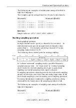
Reference
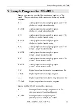
Sample software : AI1.C, AI2.C, AI3.C, AI4.C, AII.C, AII98.C
Feeding conversion data
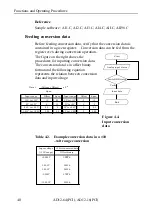
Before feeding conversion data, verify that the conversion data is
contained in a given register. Conversion data can be fed from the
register even during conversion operation.
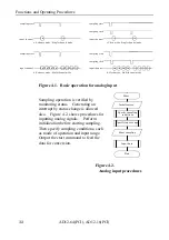
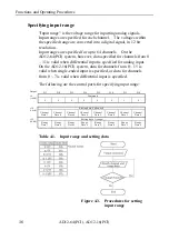
The figure on the right shows the
procedures for inputting conversion data.
The conversion data is in offset binary
format and the following equation
represents the relation between conversion
data and input voltage:
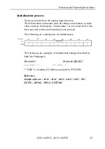
Figure 4.4.
Input conversion
data
Table 4.2. Example conversion data in a ±10
–volt range conversion
Input voltage
12-bit conversion data
(±10V range)
Offset binary
+9.995V
0FFF h
:
:
0.005V
0801 h
0.000V
0800 h
-0.005V
07FF h
:
:
-10.000V
0000 h
Verify
Input data
Verify DRE status
Start
Analog input status
End
Data =
(V Offset)
x 2
12
Span
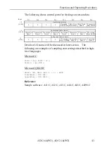
Input range
Offset
Span
Input range
Offset
Span
-10V to +10V
10
20
0V to +10V
0
10
-5V to +5V
5
10
0V to +5V
0
5
-2.5V to +2.5V
2.5
5
0V to +2.5V
0
2.5
-1.25V to +1.25V
1.25
2.5
0V to +1.25V
0
1.25
Summary of Contents for AD12-16(PCI)
Page 1: ...AD12 64 PCI AD12 16 PCI 64 16 Channel Analog to Digital Input Board for PCI User s Guide...
Page 61: ...Functions and Operating Procedures AD12 64 PCI AD12 16 PCI 54...
Page 67: ...Calibration Procedures AD12 64 PCI AD12 16 PCI 60...
Page 71: ...System Reference AD12 64 PCI AD12 16 PCI 64...
Page 74: ...Index AD12 64 PCI AD12 16 PCI...
Page 75: ...A 46 068 LZJ3711 021011 991104...


