C148GTL DX ALIGNMENT PROCEDURE
1. Test Equipment Required
a) VTVM (Fuli scalę; IV DC with RF Probe)
b) RF Output Pcwer Meter.
c) Spectrum Analyzer.
d) Frequency Counter (0-30MHz).
e) DC Pcwer Supply (13.8V, 2Amp.).
f) 50 ohm load and Attenuator.
g) Oscilloscope (0-30MHz).
h) AF Oscillator.
i) DC Anmeter.
2. Alignment Procedure
Alignment of Transmitter Section
STEP
PRESET ТО
ADJUSTMENT
PROCEDURE
1
TX. Mode.
Band SW: Mid
CH
: 19
Mode
: USB
Mic. VR: CW
CH9
: OFF
Coarse : Center
VRll
Remove PC-834 (PCB) and connect DC Am
meter to TP9(+) and TP8(-). Adjust for
50mA reading.
2
Same as Step 1.
VR10
Connect DC Ammeter to TP9(+) and TP7(-)
and adjust for 50mA reading.
3
Same as Step 1,
except Mic input
30mV.
VR12
L53
Restore PC-834. T u m VR12 to Mac. CW.
and t u m the core of L53 to the obttcm.
4
Same as Step 3.
L52, 54, 55
Adjust for Max. reading on RF VTVM.
5
Same as Step 3.
L53
Set the Band: HI, CH40. And adjust for
Max. reading on RF VTVM, then t u m the
Band: 1 Ш , CH 1, readjust for mimimum
différence in output pcwer.
6
Same as Step 1,
except;
Mode
: AM
Mic input 90% mod
L44
Adjust for Max. reading on RF VTVM.
38
Summary of Contents for 148GTL-DX
Page 32: ...со SO AOJ VR2 BLOCK DI AGRAM ...
Page 33: ...SCHEMATIC DIAGRAM ...
Page 41: ...Parts Layout Top View Î37 2SB525C 1 4 1 5 ...
Page 42: ...PARTS LAYOUT Top View ...
Page 43: ...ADDED PARTS MAIN PCB Bottom View PC 879AB ...
Page 44: ...COPPER PATTERN SWR PCB CH SW PCB LED PCB CD ...
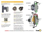
Page 48: ...го w INTERNAL DIAGRAM IC s MB87I9 ...
Page 49: ...INTERNAL DIAGRAM IC s го А ...
Page 50: ...INTERNAL DIAGRAM IC s S 0 4 2 P 25 ...
Page 58: ...со го BLOCK DI AGRAM ...
Page 59: ...PB OIO SCHEMATIC DIAGRAM ...
Page 60: ...WiRING DIAGRAM 3 5 3 6 P C 881 P C 8 8 0 ...
Page 66: ...COPPER PATTERN MAIN PCB ...
Page 68: ...P B O I O ADDED PARTS MAIN PCB H fs il 8 46 ...
Page 70: ...COPPER PATTERN SUB ASSY PCB s ...
Page 71: ...PARTS LAYOUT MIC JACK 49 ...
Page 74: ...INTERNAL DIAGRAM IC s MC14008B 1 4 Cou l 13 S 4 13 S 3 11 S2 10 S 1 16 15 14 13 12 11 10 9 52 ...
Page 75: ...сл С О INTERNAL DIAGRAM IC s OSC out Г 2 out FS PO PI P2 P3 PA P5 P6 P7 P8 MC145106 ...
Page 76: ...INTERNAL DIAGRAM IC s 14 0UT4 13 I N 4 12 lN 4 11 VEE 10 IN 3 9 I N 3 8 0UT3 TA75902P 54 ...