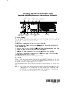
CONTROLS AND INDICATORS
There are thirteen Controls and three indicators on the front panel of your
COBRA 148GTL-DX.
Section IV
Operation
A, CONTROL FUNCTIONS
1. MIKE GAIN, (inner dual concentric) Ad justs the microphone gain in the
transmit and PA modes. This Controls the gain to the extent that fuli talk
power is available several inches away from the microphone.
2. OFF/ON/VOLUME (inner dual concentric). Turn clockwise to apply power
to the unit and to set the desired listening level. During normal CB opera
tion, the VOLUME control is used to adjust the output level obtained either
at the transceiver speaker or the extemal speaker, if used.
3. SQUELCH (outer dual concentric). This control is used to eut off or elimi-
nate receiver background noise in the absence of an incoming signal. For
maximum receiver sensitivity it is desired that the control be'Idjusted only
to the point where the receiver background noise or ambient background
noise is eliminated. Tum fully counterclockwise then slowly clockwise until
the receiver noise disappears. Any signal to be received must now be slightly
stronger than the average received noise. Further clockwise rotation will
increase the threshold level which a signal must overcome in order to be
heard. Only strong signais will be heard at a maximum clockwise setting.
4. RF GAIN CONTROL (outer dual concentric). Used to reduce the gain of
the RF amplifier under strong signal conditions.
-
12
-
Summary of Contents for 148GTL-DX
Page 32: ...со SO AOJ VR2 BLOCK DI AGRAM ...
Page 33: ...SCHEMATIC DIAGRAM ...
Page 41: ...Parts Layout Top View Î37 2SB525C 1 4 1 5 ...
Page 42: ...PARTS LAYOUT Top View ...
Page 43: ...ADDED PARTS MAIN PCB Bottom View PC 879AB ...
Page 44: ...COPPER PATTERN SWR PCB CH SW PCB LED PCB CD ...
Page 48: ...го w INTERNAL DIAGRAM IC s MB87I9 ...
Page 49: ...INTERNAL DIAGRAM IC s го А ...
Page 50: ...INTERNAL DIAGRAM IC s S 0 4 2 P 25 ...
Page 58: ...со го BLOCK DI AGRAM ...
Page 59: ...PB OIO SCHEMATIC DIAGRAM ...
Page 60: ...WiRING DIAGRAM 3 5 3 6 P C 881 P C 8 8 0 ...
Page 66: ...COPPER PATTERN MAIN PCB ...
Page 68: ...P B O I O ADDED PARTS MAIN PCB H fs il 8 46 ...
Page 70: ...COPPER PATTERN SUB ASSY PCB s ...
Page 71: ...PARTS LAYOUT MIC JACK 49 ...
Page 74: ...INTERNAL DIAGRAM IC s MC14008B 1 4 Cou l 13 S 4 13 S 3 11 S2 10 S 1 16 15 14 13 12 11 10 9 52 ...
Page 75: ...сл С О INTERNAL DIAGRAM IC s OSC out Г 2 out FS PO PI P2 P3 PA P5 P6 P7 P8 MC145106 ...
Page 76: ...INTERNAL DIAGRAM IC s 14 0UT4 13 I N 4 12 lN 4 11 VEE 10 IN 3 9 I N 3 8 0UT3 TA75902P 54 ...