C148GTL DX
GENERÄL
Channels
Frequency Range
Frequency Control
Frequency Tolérance
Frequency Stability
Operating Temerature Range
Microphone
Input Voltage
Size
Vfeight
Antenna Connector
Meter (3-in-l)
TRANSMITTER
Pcwer Output
Modulation
Intermodulation Distortion
SSB Carrier Suppression
Unwanted Sideband
Frequency Response
Output Impédance
Output Indicators
RECEIVER
Sensitivity
Selectivity
Image Rejection
SPECIFICATIONS
120FM, 120AM, 120 LSB, 120 USB, 120CW.
Lew Band, 26.515 to 26.955 MHz.
Mid Band, 26.965 to 27.405 MHz.
Hi Band, 27.415 to 27,855 MHz;
Phase Lock Loop (PLL) Synthesizer.
0.005%
0
.
001
%
-30 C to +50 C.
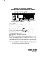
Plug-in dynamie: with push-to-talk switch
and ooiled cord.
13.8 DC nominal 15.9 max., 11.TV min.
(positive or negative ground).
Transmit: AM full mod., 2.2A.
SSB 12 watts PEP output, 2A.
Receiver: Squelched, 0.3 A.
Maximum audio output, 0.7 A.
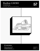
2-3/8"(H) x 7-7/8"(W) x 9-1/4"(D).
5 lbs.
UHF, S0239
Illuminated; indicates relative output power,
received signal strenght, and SWR.
AM/FM/CW, 5 watts.
SSB, 12 watts, PEP
High-and lcw-level Class B, Anplitude Modu
lation: AM, Variable capacitance Frequency
Modulation: FM.
SSB: 3rd order, more than -25 dB.
5th order, more than -35 dB.
55 dB
50 dB
AM and FM: 450 to 2500 Hz.
50 ohms, unbalanced
Meter shews relative RF output power and SWR.
Transmit LED glcws red when transmit
ter is
in operation.
O Ü D / V— »
» •
V/ •
O
V A V
A V J A
__________ %
__
greater than Ц-watt of audio output.
AM: 0.5 uV for 10 dB (S+N)/N at greater
than Ц-watt of audio output.
FM: 1.0 uV for 20 dB (S+N)/N at greater
than Ц-watt of audio output.
AM/FM: 6 dB @3 KHz, 50 dB @9 KHz.
SSB/CW: 6 dB @2.1 KHz, 60 dB @3.3 KHz.
More than 65 dB.
62
Summary of Contents for 148GTL-DX
Page 32: ...со SO AOJ VR2 BLOCK DI AGRAM ...
Page 33: ...SCHEMATIC DIAGRAM ...
Page 41: ...Parts Layout Top View Î37 2SB525C 1 4 1 5 ...
Page 42: ...PARTS LAYOUT Top View ...
Page 43: ...ADDED PARTS MAIN PCB Bottom View PC 879AB ...
Page 44: ...COPPER PATTERN SWR PCB CH SW PCB LED PCB CD ...
Page 48: ...го w INTERNAL DIAGRAM IC s MB87I9 ...
Page 49: ...INTERNAL DIAGRAM IC s го А ...
Page 50: ...INTERNAL DIAGRAM IC s S 0 4 2 P 25 ...
Page 58: ...со го BLOCK DI AGRAM ...
Page 59: ...PB OIO SCHEMATIC DIAGRAM ...
Page 60: ...WiRING DIAGRAM 3 5 3 6 P C 881 P C 8 8 0 ...
Page 66: ...COPPER PATTERN MAIN PCB ...
Page 68: ...P B O I O ADDED PARTS MAIN PCB H fs il 8 46 ...
Page 70: ...COPPER PATTERN SUB ASSY PCB s ...
Page 71: ...PARTS LAYOUT MIC JACK 49 ...
Page 74: ...INTERNAL DIAGRAM IC s MC14008B 1 4 Cou l 13 S 4 13 S 3 11 S2 10 S 1 16 15 14 13 12 11 10 9 52 ...
Page 75: ...сл С О INTERNAL DIAGRAM IC s OSC out Г 2 out FS PO PI P2 P3 PA P5 P6 P7 P8 MC145106 ...
Page 76: ...INTERNAL DIAGRAM IC s 14 0UT4 13 I N 4 12 lN 4 11 VEE 10 IN 3 9 I N 3 8 0UT3 TA75902P 54 ...