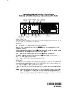
Fig. 5. Microphone plug pin numbers viewed from rear of pin réceptacle.
Be sure that the housing and the knurled ring of Fig. 3 are pushed back onto
the microphone cable before starting to solder. If the washer is not captive to
the pin réceptacle body, make sure that it is placed on the threaded portion
of the pin réceptacle body before soldering.
If the microphone jack is used to hold the pin réceptacle during the soldering
operation, best results are obtained when the connections to pins 1 and 3 are
made fïrst and then the connections to pins 2, 4 and 5. Use a minimum
amount of solder and be careful to prevent excessive solder accumulation on
pins, which could cause a short between the pin and the microphone plug
housing.
6. When ail soldering connections to the pins of the microphone plug are com
plété, push the knurled ring and the housing forward and screw the housing
onto the threaded portion of the pin receptade body. Note the location of
the screw clearance hole in the plug housing with respect to the threaded hole
in the pin réceptacle b'ody. When the housing is completely threaded into the
pin réceptacle body, a final fraction of a tiim either clockwise or counter-
clockwise may be required to align the screw hole with the threaded hole in
the pin réceptacle body. When these are aligned, the retaining screw is then
screwed into the place to secure the housing to the pin réceptacle body.
7. The two cable clamp retainer screws should now be tightened to secure the
housing to the microphone cord. If the cutting directions hâve been carefully
followed, the cable clamp should secure to. the insulating jacket of the micro
phone cable.
8. Upon completion of the microphone plug wiring, connect and secure the
microphone plug in the transceiver.
- 2 0
-
Summary of Contents for 148GTL-DX
Page 32: ...со SO AOJ VR2 BLOCK DI AGRAM ...
Page 33: ...SCHEMATIC DIAGRAM ...
Page 41: ...Parts Layout Top View Î37 2SB525C 1 4 1 5 ...
Page 42: ...PARTS LAYOUT Top View ...
Page 43: ...ADDED PARTS MAIN PCB Bottom View PC 879AB ...
Page 44: ...COPPER PATTERN SWR PCB CH SW PCB LED PCB CD ...
Page 48: ...го w INTERNAL DIAGRAM IC s MB87I9 ...
Page 49: ...INTERNAL DIAGRAM IC s го А ...
Page 50: ...INTERNAL DIAGRAM IC s S 0 4 2 P 25 ...
Page 58: ...со го BLOCK DI AGRAM ...
Page 59: ...PB OIO SCHEMATIC DIAGRAM ...
Page 60: ...WiRING DIAGRAM 3 5 3 6 P C 881 P C 8 8 0 ...
Page 66: ...COPPER PATTERN MAIN PCB ...
Page 68: ...P B O I O ADDED PARTS MAIN PCB H fs il 8 46 ...
Page 70: ...COPPER PATTERN SUB ASSY PCB s ...
Page 71: ...PARTS LAYOUT MIC JACK 49 ...
Page 74: ...INTERNAL DIAGRAM IC s MC14008B 1 4 Cou l 13 S 4 13 S 3 11 S2 10 S 1 16 15 14 13 12 11 10 9 52 ...
Page 75: ...сл С О INTERNAL DIAGRAM IC s OSC out Г 2 out FS PO PI P2 P3 PA P5 P6 P7 P8 MC145106 ...
Page 76: ...INTERNAL DIAGRAM IC s 14 0UT4 13 I N 4 12 lN 4 11 VEE 10 IN 3 9 I N 3 8 0UT3 TA75902P 54 ...