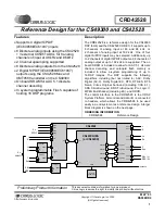


4
Figure 5. Clock and Data Connections for S/PDIF (IEC61937 / IEC60958) Input ........................ 11
Figure 6. Control and Data I/O ...................................................................................................... 16
Figure 7. DSP ................................................................................................................................ 17
Figure 8. External Memory ............................................................................................................ 18
Figure 9. CoDec ............................................................................................................................ 19
Figure 10. External A/D Converters .............................................................................................. 20
Figure 11. L/R Input Filters............................................................................................................ 21
Figure 12. Ls/Rs Input Filters ........................................................................................................ 22
Figure 13. C/Sub Input Filters ....................................................................................................... 23
Figure 14. SBL/SBR Input Filters .................................................................................................. 24
Figure 15. L/R Output Filters ......................................................................................................... 25
Figure 16. Ls/Rs Output Filters ..................................................................................................... 26
Figure 17. C/Sub Output Filters..................................................................................................... 27
Figure 18. SBL/SBR Output Filters ............................................................................................... 28
Figure 19. Top Layer ..................................................................................................................... 29
Figure 20. Bottom Layer................................................................................................................ 30
Figure 21. Assembly Drawing ....................................................................................................... 31
Figure 22. UDSP - Top .................................................................................................................. 37
Figure 23. UDSP - Digital Audio Port ............................................................................................ 38
Figure 24. UDSP - Headphone Amplifier ...................................................................................... 39
Figure 25. UDSP - Microcontroller ................................................................................................ 40
Figure 26. UDSP - Power .............................................................................................................. 41
Figure 27. UDSP - Parellel Port Interface ..................................................................................... 42
Figure 28. UDSP - RS232 Interface .............................................................................................. 43
Figure 29. UDSP - RS422 Interface .............................................................................................. 44
Figure 30. UDSP - S/PDIF I/O....................................................................................................... 45
LIST OF TABLES
Summary of Contents for CS49300
Page 16: ...16 APPENDIX D SCHEMATICS Figure 6 Control and Data I O ...
Page 17: ...17 Figure 7 DSP ...
Page 18: ...18 Figure 8 External Memory ...
Page 19: ...19 Figure 9 CoDec ...
Page 20: ...20 Figure 10 External A D Converters ...
Page 21: ...21 Figure 11 L R Input Filters ...
Page 22: ...22 Figure 12 Ls Rs Input Filters ...
Page 23: ...23 Figure 13 C Sub Input Filters ...
Page 24: ...24 Figure 14 SBL SBR Input Filters ...
Page 25: ...25 Figure 15 L R Output Filters ...
Page 26: ...26 Figure 16 Ls Rs Output Filters ...
Page 27: ...27 Figure 17 C Sub Output Filters ...
Page 28: ...28 Figure 18 SBL SBR Output Filters ...
Page 29: ...29 APPENDIX E LAYOUT PLOTS GROUND PLANE VIAS ARE FLOODED Figure 19 Top Layer ...
Page 30: ...30 Figure 20 Bottom Layer ...
Page 31: ...31 Figure 21 Assembly Drawing ...
Page 50: ......