background image

ATXP-965Q Technical Reference  

Appendix A – Technical Summary
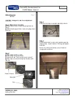
 

Chassis Plans  

49 

I/O Map 

ADDRESS MAP 

SIZE 


0000 - 00FF 

256 

RESERVED 

01F0 – 01F7 

PRIMARY PATA CHANNEL 

0228 – 022F 

LPT3 

0278 – 027F 

LPT2 

02E8 – 02EF 

COM4 

02F8 – 02FF 

COM2 

0378 – 037F 

LPT1 

03B0 – 03BB 

12 

Q965 MCH 

03C0 – 03DF 

32 

Q965 MCH 

03E8 – 03EF 

COM3 

03F0 – 03F5 

FLOPPY 

03F4 – 03F7 

PRIMARY PATA CHANNEL 

03F8 – 03FF 

COM1 

04D0 – 04D1 

PIC CONTROL 

0CF8 - 0CFB 

PCI CONF. REGISTER 

0CF9 

RESET CONTROL REGISTER 

0CFC – 0CFF 

PCI CONF. DATA REGISTER 

FFA0 – FFA7 

PRIMARY PATA BUS MASTER 


PCI Routing Table  

ATXP-965Q ISEL 

IRQx  REQ/GNT 

PCI Slot 1 

AD16 

F,G,H,E 

PCI Slot 2 

AD17 

G,F,E,H 


Summary of Contents for ATXP-965Q

Page 1: ...P 965Q Long Life Industrial Motherboard Revision A Technical Reference Intel Core 2 Duo E6400 Intel Core 2 Duo E4300 Intel Pentium 4 or Intel Celeron D 440 Embedded Processors Intel 965Q Express Chips...

Page 2: ...tion provided Chassis Plans liability shall in no event exceed the purchase price of the product purchased hereunder The foregoing limitation of liability shall be equally applicable to any service pr...

Page 3: ...y be trademarks or registered trademarks of their respective companies LIABILITY This manual is as complete and factual as possible at the time of printing DISCLAIMER however the information in this m...

Page 4: ......

Page 5: ...orm Factor and Dimensions 6 Reliability 7 Agency Approvals 7 Environmental Requirements 7 CHAPTER 2 HARDWARE CONFIGURATION 9 Handling Precautions 9 Connector Location 10 Header and Jumper Location 11...

Page 6: ...ices 52 Graphics Features 53 APPENDIX B RAID CONFIGURATION 55 Configuring for RAID Intel Matrix Storage Technology 55 Configuring the BIOS for Intel Matrix Storage Technology 55 Creating your RAID Set...

Page 7: ...sponsible for any loss or damage resulting from the use or misuse of this publication This publication and any accompanying software may not in whole or in part be copied photocopied translated or red...

Page 8: ...Index ATXP 965Q Technical Reference iv Chassis Plans This Page Intentionally Blank...

Page 9: ...processors in a LGA775 socket FC LGA4 With proper installation and maintenance your ATXP 965Q will provide years of high performance and trouble free operation This manual provides a detailed explanat...

Page 10: ...e reasonable protection against harmful interference when the equipment is operated in a commercial environment This equipment generates uses and can radiate radio frequency energy and if not installe...

Page 11: ...65nm Intel Core 2 Duo E6400 2M unified cache 800 1066 MHz FSB 65nm Intel Core 2 Duo E4300 2M unified cache 800 MHz FSB 65nm Intel Core 2 Duo E2160 2M unified cache 800 MHz FSB 65nm Intel Celeron 440...

Page 12: ...rts ACPI 3 0 Support 652 mBGA package Peripheral Chips SMSC SCH3114 SIO chip Four full handshake COM ports IRDA on 6 pin header Floppy parallel keyboard mouse Hardware voltage monitor CPU temp monitor...

Page 13: ...serial ports Shared infrared support IRDA 1 0 Compliant on COM2 Two 2 additional serial ports on 2 10 pin shrouded headers 6 pin IRDA header USB Interfaces 10 4 USB ports on 2 shared RJ45 Doubled stac...

Page 14: ...ader Reset Soft Power LEDs for power and HDD CPU Socket 775 pin LGA Power connectors ATX2 2 24 pin power connector backwards compatible with 20 pin 8 pin ATX12V power connector backward compatible wit...

Page 15: ...pprovals FCC CE Certification Please contact your local Regional Sales Manager for the certificate Environmental Requirements RoHS compliant assembly CATEGORY OPERATING NON OPERATING TEMPERATURE 0 C t...

Page 16: ...Chapter 1 Technical Specifications ATXP 965Q Technical Reference 8 Chassis Plans This Page Intentionally Blank...

Page 17: ...so occur by using excessive force in performing certain installation procedures such as forcing the system board into the chassis or placing too much torque on a mounting screw Take special care when...

Page 18: ...ss x16 Serial ATA2 Connector SATA1 2 3 4 5 6 ATX Power Connector Floppy Connector LAN 2 USB J8 LAN 1 USB J7 DDR2 Channel 1 PCI Express x4 x16 PS 2 Keyboard Mouse J3 COM1 COM2 J5 VGA AUDIO J7 775 CPU S...

Page 19: ...imary IDE Slave SATA 1 J11 Secondary IDE Slave SATA 1 J14 Third IDE Master SATA 2 J13 Fourth IDE Master SATA 2 Header and Jumper Location USB2 3 USB0 1 USB8 9 Front Panel IR J22 TPM Module J21 SYS_ FA...

Page 20: ...nnector 34 pin shrouded header SATA1 6 J9 J10 J11 J12 J13 J14 Serial ATA2 Port Connector 7 pin shrouded connector Header Name Description AUDIO Line Out MIC Headers 10 pin keyed header EXT_USB 0 1 J23...

Page 21: ...ion information There are two different categories of jumpers on the ATXP 965Q A Two pin jumpers are used for binary selections such as enable disable Instructions for this type of jumper are open for...

Page 22: ...CMOS Reset This option is provided as a convenience for those who need to reset the CMOS registers It should always be set to Normal for standard operation If the CMOS needs to be reset turn off the s...

Page 23: ...DIMM PCS Total Memory Bank 0 1 DIMM1 DDR2 533 DDR2 667 DDR2 800 X1 128MB 2 0GB Bank 2 3 DIMM2 DDR2 533 DDR2 667 DDR2 800 X1 128MB 2 0GB Bank 4 5 DIMM3 DDR2 533 DDR2 667 DDR2 800 X1 128MB 2 0GB Bank 6...

Page 24: ...socket lever by pushing the lever down and away from the socket 2 Lift the metal plate and make sure not to touch the socket pins 3 Remove the plastic protective cover 1 Improper installation of the C...

Page 25: ...l not to touch the bottom contacts of the processor 5 Hold the processor as shown in the picture Align the processor with the socket A Align the processor notches B with the socket C Insert the proces...

Page 26: ...he fan s plug to the board taking into consideration the polarity of connector CPU_FAN CPU Fan connector The pin assignment is as follows PIN ASSIGNMENT 1 GND 2 12V 3 Tachometer 4 PWM SYS_FAN and NB_F...

Page 27: ...ATX 12V Specification 2 0 or better compliant power supply unit PSU with a minimum of 350W power rating is recommended This type has 24 pin and 4 pin power plugs If you intend to use a PSU with 20 pi...

Page 28: ...section for more information VGA Connector 15 pin D Sub Connector VGA J5A The 15 pin D Subminiature female connector supports analog displays Audio Line In Lin Out MIC Connector AUDIO J5B The 3 color...

Page 29: ...r the support of up to 6 SATA devices It is preferable to use SATA II certified cables These cables easily connect to the motherboard and the SATA peripheral Line Out MIC Header 9 pin AUDIO These head...

Page 30: ...at other end to the floppy drives If using a single drive make sure to connect it to the connector at the end of the cable Floppy Drive Connector Pin 1 FDD USB Port Headers 9 pin USB0 1 USB2 3 USB8 9...

Page 31: ...le Headers IR Pin1 G ND IR RX NC VC C 5 IRTX 2 5 6 AUX CD Audio In and CD Audio In Headers 4 pin J18 AUX_CDIN J15 CD IN AUX_CDIN and CD IN are the connectors for auxiliary CD signals AUX CD Audio In H...

Page 32: ...assis Plans PRINTER PORT J20 Pi n 1 Serial COM Port COM3 COM4 COM3 COM4 are available through 9 pin shrouded headers These ports can be disabled or configured through BIOS SETUP Please refer to Chapte...

Page 33: ...ST_BTN Power LED PWR LED Connect your system Power LED to these pins Connect a bi color LED for additional functionality signaling not supported PIN ASSIGNMENT 2 PW_LED 4 PW_LED Power Button PWR BTN T...

Page 34: ...his allows for 3 5 times the bandwidth of the AGP8X and it supports a peak concurrent bandwidth of 8Gbyte sec at full speed Five 32 bit PCI slots guarantee the rich connectivity for peripheral I O Fou...

Page 35: ...to indicate the failure of a critical system component during this time Consult Appendix B for a list of Beep codes used by the BIOS Starting BIOS Setup AMIBIOS has been integrated into many motherbo...

Page 36: ...or sub screen Plus Minus The Plus and Minus Arrow keys allow you to change the field value of a particular setup item For example Date and Time Tab The Tab key allows you to select setup fields Note...

Page 37: ...ion and exit You can also use the Arrow key to select Cancel and then press the Enter key to abort this function and return to the previous screen ESC The Esc key allows you to discard any changes you...

Page 38: ...row keys Enter new values through the keyboard Press the Tab key or the Arrow keys to move between fields The date must be entered in MM DD YY format The time is entered in HH MM SS format Note The ti...

Page 39: ...es in below Sections may cause system to malfunction CPU Configuration IDE Configuration Floppy Configuration Super IO Configuration Hardware Health Configuration ACPI Configuration AHCI Configuration...

Page 40: ...the IDE devices The CMOS screen is showing you the two SATA Host Controllers 1 2 where SATA controller 1 controls the first 4 SATA ports and SATA 2 control the last 2 SATA ports Below are the options...

Page 41: ...selects the I O address used by the parallel port Available options are Disabled 378 278 and 3BC Parallel Port Mode This option selects the parallel port mode Available options are Normal SPP Bi Dir E...

Page 42: ...used to pass POST data to the AML code during ACPI O S operations Headless Mode Enable or Disable This option is used to update the ACPI FACP table to indicate headless operations Chipset ACPI Configu...

Page 43: ...re Redirection after BIOS POST Disable Turn off the redirection after POST Boot Loader Redirection is active during Boot loader Always Redirection is always active some OS s may not work if set to alw...

Page 44: ...assis Plans USB Mass Storage Device Configuration Emulation Type Auto Floppy Forced FDD HDD CDROM If Auto USB devices less than 530 MB will be emulated as Floppy and remaining as HDD Forced FDD option...

Page 45: ...Enabled Off Board PCI ISA IDE Card Auto IRQ3 Available IRQ4 Available IRQ5 Available IRQ7 Available IRQ9 Available IRQ10 Available IRQ11 Available IRQ14 Available IRQ15 Available DMA Channel 0 Availab...

Page 46: ...lled in the system It does this so the ISA based Graphics card will function correctly This does not necessarily indicate a physical ISA adapter card The graphics chipset can be mounted on a PCI card...

Page 47: ...alue to allow the system to reserve 64K of the system memory to the ISA devices Reserved Memory Address Note Reserved Memory Address can be displayed and set manually only if the Reserved Memory Size...

Page 48: ...tically when the computer system is boot up PS 2 Mouse Support Disabled This option will prevent the PS 2 mouse port from using system resources and will prevent the port from being active Use this se...

Page 49: ...gory type such as Hard disk drives Removable media or ATAPI CD ROM devices from the boot menu For example if the 1st boot device is set to Hard disk drives then BIOS will try to boot to hard disk driv...

Page 50: ...rd security If you select password support you are prompted for a one to six character password Type the password on the keyboard The password does not appear on the screen when typed Make sure you wr...

Page 51: ...rd has been set if the password has been installed Installed displays If not Not Installed displays User Password Indicates whether a user password has been set If the password has been installed Inst...

Page 52: ...85 2006 American Mega trends Inc Northbridge Configuration Memory Remap Feature Enabled Allows remapping of overlapped PCI memory above the total physical memory Disabled Does not allow remapping PCI...

Page 53: ...Enables or Disabled SMBUS Controller SLP_S4 Min Assertion Width Select 1 2 2 3 3 4 and 4 5 Restore on AC Power Loss Selects how the ATXP 965Q behaves after power loss Options are Power Off Power On a...

Page 54: ...nt changes to the system configuration Load Optimal Defaults This option automatically sets all CMOS Setup options to a complete set of default settings The Optimal settings are designed for maximum a...

Page 55: ...LLER HUB VGA 533 800 1066 MHz FSB HD Audio CODEC VGA Connector DDR2 SDRAM 4 MODULES 8GB Max Single Dual Ch PCI v 2 3 VRD 11 DC to DC Vcore 82573L PCI E 10 100 1000 ETHERNET MAC PHY RJ45 MAGJACK Connec...

Page 56: ...RUNTIME BIOS 896K 960K E0000 EFFFF 64K RESERVED 800K 896K C8000 DFFFF 96K AVAILABLE TO ADAPTER ROMS 640K 800K A0000 C7FFF 160K VIDEO MEMORY AND BIOS 639K 640K 9FC00 9FFFF 1K EXTENDED BIOS DATA 512K 6...

Page 57: ...02FF 8 COM2 0378 037F 8 LPT1 03B0 03BB 12 Q965 MCH 03C0 03DF 32 Q965 MCH 03E8 03EF 8 COM3 03F0 03F5 6 FLOPPY 03F4 03F7 4 PRIMARY PATA CHANNEL 03F8 03FF 8 COM1 04D0 04D1 2 PIC CONTROL 0CF8 0CFB 4 PCI...

Page 58: ...2 00 INTEGRATED GRAPHICS 00 1B 00 HD AUDIO 00 1D 00 UHCI 00 1D 01 UHCI 00 1D 02 UHCI 00 1D 03 UHCI 00 1A 07 UHCI 00 1A 07 EHCI 00 1D 07 EHCI 00 1E 00 PCI BRIDGE 00 1F 00 LPC 00 1F 02 SATA 1 00 1F 05 S...

Page 59: ...N A Programmable Interrupt 3 8 Communications Port COM2 4 9 Communications Port COM1 5 6 Optional LPT2 6 11 Floppy Disk Controller 7 7 Printer Port LPT1 8 N A System CMOS Real Time Clock 9 10 ACPI Mod...

Page 60: ...display is connected Please refer to Appendix B for POST codes description On board Ethernet The ATXP 965Q features two Intel 82573L Ethernet Controllers PCIe x1 PCIe interface Peak bandwidth 2Gb s p...

Page 61: ...s via the PCI Express Graphics PEG port but cannot work concurrently with the integrated graphic device SDVO and Analog Display Features The GMCH provides interfaces to a progressive scan analog monit...

Page 62: ...Card Support The GMCH routes two multiplexed DVO ports that are each capable of driving up to a 200 MHz pixel clock to the PCI Express x16 connector The DVO ports can be paired for a dual channel con...

Page 63: ...e available RAID 5 and RAID 10 these options will only appear if three or four SATA drives are installed respectively Press Enter once you have selected the RAID LEVEL 4 Select the drives to be used i...

Page 64: ...Appendix B Raid Configuration ATXP 965Q Technical Reference 56 Chassis Plans This Page Intentionally Blank...

Page 65: ...ve a circular pad Q COM1 The pin assignment is as follows PIN ASSIGNMENT RS 232 RS 485 RS 422 1 COM1_DCD TX TX 2 COM1_RX TX TX 3 COM1_TX RX RX 4 COM1_DTR RX RX 5 GND GND GND 6 COM1_DSR GND RTS 7 COM1_...

Page 66: ...in assignment is as follows PIN ASSIGNMENT 1 COM3_DCD 2 COM3_RX 3 COM3_TX 4 COM3_DTR 5 GND 6 COM3_DSR 7 COM3_RTS 8 COM3_CTS 9 COM3_RI COM4 COM4 is fixed as RS 232 The pin assignment is as follows PIN...

Page 67: ...r The pin assignments are as follows PIN ASSIGNMENT 1 SIN2 2 GND 3 GND 4 NC 5 SOUT2 6 5VDU Universal Serial Bus Header J23 J24 and J25 Universal Serial Bus Connectors The pin assignments are as follow...

Page 68: ...MENT 1 RED 2 GREEN 3 BLUE 4 VCC 5 GND 6 GND 7 GND 8 GND 9 VCC 10 GND 11 VCC 12 5VCDA 13 HSYNC 14 VSYNC 15 CLK Serial ATA Connector J9 J10 J11 J12 SATA 1 Port Connectors J13 J14 SATA 2 Port Connectors...

Page 69: ...connect up to two FDDs to the ATXP 965Q The pin out is as follows PIN ASSIGNMENT PIN ASSIGNMENT 1 GND 2 F_DENSEL 3 GND 4 NC 5 GND 6 Key 7 GND 8 F_INDEX 9 GND 10 F_MTRA 11 GND 12 F_DRVB 13 GND 14 F_DR...

Page 70: ...s PIN ASSIGNMENT PIN ASSIGNMENT 1 STROBE 14 GND 2 AUTOFEED 15 DATA BIT 6 3 DATA BIT 0 16 GND 4 ERROR 17 DATA BIT 7 5 DATA BIT 1 18 GND 6 INIT 19 ACK1 7 DATA BIT 2 20 GND 8 SLCT IN 21 BUSY 9 DATA BIT 3...

Page 71: ...IGNMENT PIN ASSIGNMENT 1 3 3V 13 3 3V 2 3 3V 14 12V 3 GND 15 GND 4 5V 16 PSON 5 GND 17 GND 6 5V 18 GND 7 GND 19 GND 8 POK 20 5V 9 5VSB 21 5V 10 12V 22 5V 11 12V 23 5V 12 3 3V 24 GND CD IN AUX CD IN Co...

Page 72: ...l Header Pin Front Panel Header 1 HDD LED Anode 2 Power LED Green 3 HDD LED Cathode 4 Power LED Yellow 5 Reset GND 6 Power Switch 7 Reset 8 Power Switch GND 9 5V 10 NC SPI CON J16 Pin SPI CON J16 1 SP...

Page 73: ...zation portion of the BIOS Checkpoint Description Before D0 If boot block debugger is enabled CPU cache as RAM functionality is enabled at this point Stack will be enabled from this point D0 Early Boo...

Page 74: ...s to occur because the user has forced the update or the BIOS checksum is corrupt The following table describes the type of checkpoints that may occur during the Boot block recovery portion of the BIO...

Page 75: ...re based on CMOS setup questions Initializes both the 8259 compatible PICs in the system 05 Initializes the interrupt controlling hardware generally PIC and interrupt vector table 06 Do R W test to CH...

Page 76: ...RTC date time 3B Test for total memory installed in the system Also Check for DEL or ESC keys to limit memory test Display total memory in the system 3C Mid POST initialization of chipset registers 40...

Page 77: ...on 2A Initialize different buses and perform the following functions Reset Detect and Disable function 0 Static Device Initialization function 1 Boot Output Device Initialization function 2 Function 0...

Page 78: ...erned 3 func 3 input device initialization on the BUS concerned 4 func 4 IPL device initialization on the BUS concerned 5 func 5 general device initialization on the BUS concerned 6 func 6 error repor...

Page 79: ...p codes used by AMIBIOS Table B 6 AMIBIOS Beep Codes Boot Block Beep Codes Number of Beeps Description 1 No media present Insert diskette in floppy drive A 2 AMIBOOT ROM file not found in root directo...

Page 80: ...unctioning add in card Remove all expansion cards except the video adapter If beep codes are generated when all other expansion cards are absent consult your system manufacturer s technical support If...

Reviews: