background image


AW86225 

October  2021  V1.9 


www.awinic.com

                                                    8                          Copyright © 2020 SHANGHAI AWINIC TECHNOLOGY CO., LTD 


Measurement Setup 

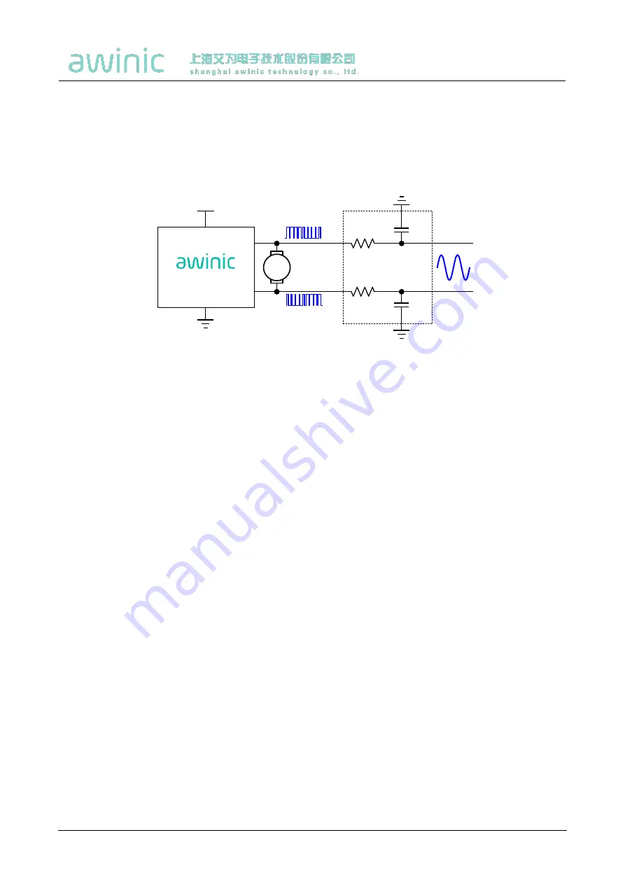
AW86225 features switching digital output, as shown in Figure 6. Need to connect a low pass filter to HDP/HDN 

output respectively  to filter  out switch modulation frequency, then measure the  differential output of filter to 

obtain analog output signal. 


HDP

HDN

AW86225

3.4kHz

Low-Pass Fliter

100k

Ω

100k

Ω

0.47nF

0.47nF

LRA


Figure 6   AW86225 test setup 

awinic Confidential

Summary of Contents for AW86225

Page 1: ...ack and hardware pin trigged playback with fast start up time All these make the AW86225 an ideal candidate for haptic driver AW86225 integrates a 3KByte SRAM for user defined waveforms to achieve a v...

Page 2: ...I O Multi mode pin Selectable as input trigger pulse or output interrupt Default function is INTN when set as interrupt output there must be a pullup resistance to be added B1 SDA I O I2C bus data inp...

Page 3: ...control Auto brake F0 tracking SRAM HSRC BEMF Detection LRA Diagnosis Figure 2 FUNCTIONAL BLOCK DIAGRAM Typical Application Circuits VDD AW86225 VDD TRIG INTN HDP HDN GND C3 10uF C2 0 1uF VREG C1 0 1...

Page 4: ...e same layer with the AW86225 chip 2 For the sake of driving capability the power lines especially the one to VDD and output lines should be short and wide as possible Ordering Information Part Number...

Page 5: ...TE 2 3 HBM Human Body Model 2KV CDM Charge Device Model 1 5KV Latch up Test Condition JEDEC EIA JESD78E IT 200mA IT 200mA NOTE 1 Conditions out of those ranges listed in absolute maximum ratings may c...

Page 6: ...RSTN 0V 0 1 1 A ISTBY Standby current RSTN 1 8V 3 A IQ Quiescent current 1 mA UVP Under voltage protection voltage 2 7 V Under voltage protection hysteresis voltage 100 mV TSD Over temperature protect...

Page 7: ...ime 0 3 0 12 s 6 tSU STA Setup time SCL to START state 0 6 0 26 s 7 tHD STA Repeat start Start condition hold time 0 6 0 26 s 8 tSU STO Stop condition setup time 0 6 0 26 s 9 tBUF the Bus idle time ST...

Page 8: ...output as shown in Figure 6 Need to connect a low pass filter to HDP HDN output respectively to filter out switch modulation frequency then measure the differential output of filter to obtain analog...

Page 9: ...LTD Typical Characteristics Figure 7 Standby Current Vs Supply Voltage Figure 9 Trig Application Figure 8 LRA with Automatic Braking Figure 10 Automatic Resonance Tracking 1 1 5 2 2 5 3 3 5 2 5 3 3 5...

Page 10: ...d no wave is going Power supply is ready and RSTN is tie to high Most parts of the device are power down for low power consumption except I2C interface and LDO Active Playing a waveform Most parts of...

Page 11: ...library in SRAM Device will be switched to this mode after haptic waveform playback finished Active Mode The device is fully operational in this mode H bridge driver circuits will start to work Users...

Page 12: ...RAM MODE TRIG MODE RTP MODE Set EN_RAMINIT 0 Global configuration Receive a Playback Request Write data to RTP FIFO Figure 13 Power up and playback sequence Software Reset Writing 0xAA to register SR...

Page 13: ...t and the braking effect becomes worse especially for short vibration waveforms So it s necessary to perform consistency calibration of LRA Firstly the power on f0 detection can be launched to get the...

Page 14: ...veform library version waveform header and waveform data 0 BFF Action1 Action127 WAV DATA WAVFORM HEADER BASE_ADDR Waveform version Start address high Start address low End address high End address lo...

Page 15: ...n blocks contain the start address 2 bytes and end address 2 bytes So the total length of waveform header block are N 4 bytes The start address contains the location in the memory where the waveform d...

Page 16: ...til all eight IDs are played whichever comes first The waveform ID is a 7 bit number The MSB of each ID register can be used to implement a delay between queue waveforms When the MSB is high bits 6 0...

Page 17: ...Playback steps Prepare RTP data before playback Set PLAY_MODE bit to 1 in register 0x08 Set GO bit to 1 in register 0x09 to trigger waveform playback Delay 1ms Check GLB_STATE 4 b1000 if HOST don t se...

Page 18: ...P TRG1SEQ_N 1 0 X X High level TRG1SEQ_P 1 X X Low level TRG1SEQ_N Playback steps Waveform library must be initialized before playback Set INTN_PIN bit to 0 in register 0x44 Set trigger playback regis...

Page 19: ..._STATE 0 Device will be switched to STANDBY mode after haptic waveform playback finished Tracking DRV1_TIME 4 DRV2_TIME 5 DRV1_LVL DRV2_LVL 4 3 2 1 1 2 3 4 5 Figure 19 Cont mode playback Auto Brake En...

Page 20: ...onitors the VDD level to ensure that is above threshold 2 7V In the event of a VDD drop the device immediately power down the H bridge driver and latches the UVLO flag Drive Data Error Protection DDEP...

Page 21: ...22 START S SDA SCL STOP P Figure 22 START and STOP state generation process In the data transmission process when the clock line SCL maintains a high level the data line SDA must remain the same Only...

Page 22: ...ly If the master device needs to continue transmitting data by sending another pair of data bytes just need to repeat the sequence from step 6 In the latter case the targeted register address will hav...

Page 23: ...after sent each acknowledge bit ACK The master device generates the STOP state to end the data transmission START slave device address R W A Register address A Read data STOP A 0 write From the maste...

Page 24: ...OOP 0x00 0x16 WAVCFG13 RW WAITSLOT MAINLOOP 0x00 0x18 CONTCFG1 RW EDGE_FRE EN_F0_DET SIN_MODE 0xE1 0x19 CONTCFG2 RW F_PRE 0x8D 0x1A CONTCFG3 RW DRV_WIDTH 0x6A 0x1C CONTCFG5 RW BRK_GAIN 0x08 0x1D CONTC...

Page 25: ...RO 1 Over Current status 0 1 OTS RO 1 Over Temperature status 0 0 DONES RO 1 The indication of playback 0 SYSINT Address 02h Bit Symbol R W Description Default 7 6 Reserved RC Not used 0 5 UVLI RC Wh...

Page 26: ...sed 0 5 STOP_MODE RW 0 stop when current wave is over 1 stop right now 0 4 3 Reserved RW Not used 0 2 BRK_EN RW When set 1 enable auto brake after RTP RAM CONT playback mode is stopped 1 1 0 PLAY_MODE...

Page 27: ...o 1 WAVSEQ8 means wait time else means wave sequence number 0 6 0 WAVSEQ8 RW Wait time code WAITSLOT or wave sequence number 0 WAVCFG9 Address 12h Bit Symbol R W Description Default 7 4 SEQ1LOOP RW Co...

Page 28: ...ay code 1 time b1111 playback infinitely until STOP set to 1 or MAINLOOP 0xF 0 CONTCFG1 Address 18h Bit Symbol R W Description Default 7 4 EDGE_FRE RW Define the edge frequency b1000 200Hz b1001 210Hz...

Page 29: ...Fh Bit Symbol R W Description Default 7 0 DRV1_TIME RW Number of half cycle for the first cont drive 4 CONTCFG9 Address 20h Bit Symbol R W Description Default 7 0 DRV2_TIME RW Number of half cycle for...

Page 30: ...FO_AEH RW High four bits of RTP FIFO almost empty threshold FIFO_AE FIFO_AEH 256 FIFO_AEL 0x02 3 0 FIFO_AFH RW High four bits of RTP FIFO almost full threshold FIFO_AF FIFO_AFH 256 FIFO_AFL 0x06 RTPCF...

Page 31: ...served RW Not used 0 GLBVFG2 Address 3Ch Bit Symbol R W Description Default 7 0 START_DLY RW Startup delay time unit time is 1 48k s 4 GLBCFG4 Address 3Eh Bit Symbol R W Description Default 7 6 GO_PRI...

Page 32: ...tion Default 7 WAKE RW Chip enable control 1 force the chip to enter active mode 0 6 STANDBY RW Chip disable control 1 force the chip to enter standby mode 0 5 4 Reserved RW Not used 2 3 INTN_PIN RW M...

Page 33: ...et protection voltage of output signal protection mode of pwm 0x3F PWMCFG4 Address 4Fh Bit Symbol R W Description Default 7 0 PRTIME RW Set protection time of input signal protection mode of pwm unit...

Page 34: ...eserved RW Not used 0 5 0 TRIM_LRA RW Register LRA trim setting Trimming OSC frequency adaptive for LRA resonant frequency deviation rate 0 18 0 26 b000000 LRA 1 0 LRA real resonant frequency b000001...

Page 35: ...age OUTPUT BEADS CAPACITORS The device output is a square wave signal which causing switch current at the output capacitor increasing static power consumption and therefore output capacitor should not...

Page 36: ...ded to reserve a combination of beads and capacitors to prevent EMI problems The default bead is 0 and the capacitor is not connecting 2 The power supply flows through C2 and C3 to the VDD pin of the...

Page 37: ...23 1 23 0 69 2 00 4 00 4 00 8 00 Q1 P2 QUADRANT ASSIGNMENTS FOR PIN 1 ORIENTATION IN TAPE TAPE DIMENSIONS A0 Dimension designed to accommodate the component width B0 Dimension designed to accommodate...

Page 38: ...ackage Description 1 127 0 020 1 127 0 020 PIN 1 CORNER Top View 0 380 0 015 0 177 0 020 0 592 MAX BALL TYP 0 1635 REF 0 800 TYP 0 400 TYP 0 800 TYP 0 400 TYP 0 1635 REF A B C 9X 0 240 0 020 1 2 3 Sid...

Page 39: ...OLOGY CO LTD Land Pattern Data METAL SOLDER MASK OPENING 0 05 MAX ALL AROUND NON SOLDER MASK DEFINED SOLDER MASK DEFINED 0 05 MAX ALL AROUND SOLDER MASK OPENING METAL UNDER SOLDER MASK UNIT mm 0 400 T...

Page 40: ...ruary 2021 Modify SRST 0x00 Register Detailed Description V1 4 March 2021 Modify LRA Resistance Detect V1 5 April 2021 Modify Pin Definition V1 6 June 2021 Modify Register Configuration and Waveform l...

Page 41: ...ogy products in such equipment or applications and therefore such inclusion and or use is at the customer s own risk Applications that are described herein for any of these products are for illustrati...

Reviews: