NV-266XC User Manual
24
1
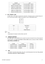
+DC12V
2
+DC12V
3
Ground
4
Ground
5
BKLT_EN
6
BKLT_CTRL
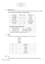
Note:
Pin6 is backlight control signal, support DC or PWM mode, mode select at BIOS CMOS menu.
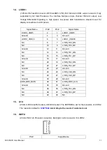
17. LVDS2
(option)
:
(1.25mm Pitch 2x20 Connector, DF13A-40DP-1.25V), For 18/24-bit LVDS2 output connector, Fully
supported by Parad PS8625(DP to LVDS), the interface features dual channel 24-bit output. Low
Voltage Differential Signaling, A high speed, low power data transmission standard used for
display connections to LCD panels.
Signal Name
Pin#
Pin#
Signal Name
LVDS2_VDD5
2
1
LVDS2_VDD5
Ground
4
3
Ground
LVDS2_VDD33
6
5
LVDS2_VDD33
LB_D0_N
8
7
LA_D0_N
LB_D0_P
10
9
LA_D0_P
Ground
12
11
Ground
LB_D1_N
14
13
LA_D1_N
LB_D1_P
16
15
LA_D1_P
Ground
18
17
Ground
LB_D2_N
20
19
LA_D2_N
LB_D2_P
22
21
LA_D2_P
Ground
24
23
Ground
LB_CLKN
26
25
LA_CLKN
LB_CLKP
28
27
LA_CLKP
Ground
30
29
Ground
LVDS2_DDC_DATA
32
31
LVDS2_DDC_CLK
Ground
34
33
Ground
LB_D3_N
36
35
LA_D3_N
LB_D3_P
38
37
LA_D3_P
NC
40
39
NC
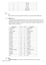
19. BTN:
POWER on/off Button
, They are used to connect power switch button. The two pins are
Summary of Contents for NV-266 C Series
Page 7: ...NV 266XC User Manual 7 Figure 1 1 Dimensions of NV 2663C ...
Page 8: ...NV 266XC User Manual 8 Figure 1 2 Dimensions of NV 2664C ...
Page 9: ...NV 266XC User Manual 9 Figure 1 3 Dimensions of NV 2665C ...
Page 12: ...NV 266XC User Manual 12 Figure 1 9 Rear view of NV 2665C ...
Page 16: ...NV 266XC User Manual 16 2 2 Board Dimensions ...
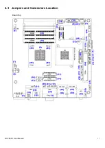
Page 17: ...NV 266XC User Manual 17 2 3 Jumpers and Connectors Location Board Top ...
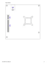
Page 18: ...NV 266XC User Manual 18 Board Bottom ...
Page 66: ...NV 266XC User Manual 66 Step 3 Click I agree Step 4 Click Continue Anyway ...
Page 67: ...NV 266XC User Manual 67 Step 5 Click Continue Anyway Step 6 Click Yes to restart the computer ...


