background image

UG-1757 

EVAL-AD5413SDZ

 Evaluation Board User Guide 


Rev. 0 | Page 4 of 17 

SOFTWARE QUICK START PROCEDURES 

INSTALLING THE 

ACE

 SOFTWARE AND  

EVAL-AD5413SDZ PLUGINS 

The EVAL-AD5413SDZ board uses Analog Devices, Inc., 

ACE


software. For instructions on how to install and use th

ACE


software, go to 

www.analog.com/ACE

.  

When the installation is finished, the EVAL-AD5413SDZ 
plugin appears when th

ACE

 software is opened.  

INITIAL SETUP 

To set up the EVAL-AD5413SDZ, take the following steps: 

1.


Connect a USB cable to the PC and then to the 

SDP-S

 board. 

2.


Connect the 

SDP-S

 board to the EVAL-AD5413SDZ. The 

PC recognizes the EVAL-AD5413SDZ. 

3.


Power up the EVAL-AD5413SDZ with the power supplies 
recommended in the Power Supplies section.  

4.


Open the 

ACE

 software. The EVAL-AD5413SDZ appears 

in the 

Attached Hardware

 pane of the 

ACE

 window. 

5.


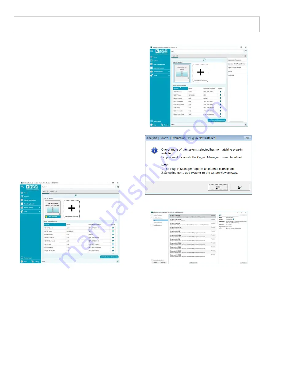
When setting up the EVAL-AD5413SDZ for the first time, 
you may be required to install the EVAL-AD5413SDZ 
plugin. If the plugin appears as shown in Figure 2, proceed 
to Step 7. If the plugin appears as shown in Figure 3, 
double-click the evaluation board symbol, and the pop-up 
window shown in Figure 4 appears. Click 

Yes

.  

23

146

 -

0

05


Figure 2. Attached Hardware Section with the EVAL-AD5413SDZ  

Plugin Connected 

23

14

6 -

0

02


Figure 3. EVAL-AD5413SDZ Plugin Not Installed 

2

3

1

46 -

003


Figure 4. Installing the Plugin Pop-Up Window 

6.


The plugin manager window appears, as shown in Figure 5. 

23

146

 -

0

0

4


Figure 5. Plugin Manager Window  

7.


Find and select the 

Board.AD5413

 plugin and click 

Install 

Selected

. The EVAL-AD5413SDZ plugin is now installed 

and displays as shown in Figure 2. In Figure 5 only, the 

AD5413

 is synonymous with the 

AD5423

.  

8.


Double-click 

EVAL-AD5413SDZ

 to open th

AD5413

 block 

diagram (see Figure 7). The 

INITIAL CONFIGURATION


window appears on the left side of the 

ACE

 window. Several 

register settings can be configured in this pane and are 
written to the device in the appropriate order. The 

RESET_OCCURED

 and 

CAL_MEM_UNREFRESHED


LED indicators in the 

DIGITAL DIAGNOSTIC RESULTS


section are illuminated red by default (see Figure 7). 

Summary of Contents for EVAL-AD5413SDZ

Page 1: ...nector cables PC or laptop DOCUMENTS NEEDED AD5413 data sheet ACE user manual SOFTWARE NEEDED ACE software GENERAL DESCRIPTION This user guide describes the EVAL AD5413SDZ for the AD5413 single channel 14 bit voltage and 14 bit current output digital to analog converter DAC The EVAL AD5413SDZ see Figure 1 requires the EVAL SDP CS1Z system demonstration platform SDP S board The EVAL AD5413SDZ inter...

Page 2: ...al Communication 3 AD5413 Device Address Pins 3 Software Quick Start Procedures 4 Installing the ACE Software and EVAL AD5413SDZ Plugins 4 Initial Setup 4 AD5413 Block Diagram and Functions 6 Initial Configuration 8 Setting the DAC Output 8 Updating Diagnostic Results 8 Example Sequences 8 ACE Tool Views 10 Macro Tool 10 Register Debugger Tool 10 Events Tool 10 Evaluation Board Schematics and Artw...

Page 3: ... supply for the ADR4525 is 15 V JP8 Inserted Connects the VIOUT pin to the VSENSE pin JP10 Inserted Connects the VSENSE pin to the RETURN signal on the EVAL AD5413SDZ JP11 A Position A connects the LDAC pin to the ground position Position B connects the LDAC pin to the VLOGIC pin JP12 A Position A connects the AD0 pin to the ground position Position B connects the AD0 pin to the VLOGIC pin JP14 A ...

Page 4: ...DZ plugin If the plugin appears as shown in Figure 2 proceed to Step 7 If the plugin appears as shown in Figure 3 double click the evaluation board symbol and the pop up window shown in Figure 4 appears Click Yes 23146 005 Figure 2 Attached Hardware Section with the EVAL AD5413SDZ Plugin Connected 23146 002 Figure 3 EVAL AD5413SDZ Plugin Not Installed 23146 003 Figure 4 Installing the Plugin Pop U...

Page 5: ...ce is power cycled or if the USB cable is disconnected and reconnected while the ACE software is open contact with the EVAL AD5413SDZ is lost To regain contact click the System tab click the USB symbol on the SDP S and then click Acquire see Figure 6 23146 106 Figure 6 Reconnecting the USB 23146 006 Figure 7 AD5413 Block Diagram in the ACE Software ...

Page 6: ...e the software default values to the hardware F The AD0 and AD1 check boxes set the AD5413 address of the device and must correspond to the JP12 and JP14 links on the hardware If either check box is selected this represents a high state If either box is not selected this represents a low state G If the RESET check box is selected the SDP S board sets the RESET pin high Otherwise the SDP S board pu...

Page 7: ...ated pop up menu K2 GP Config When this button is clicked a pop up menu appears to configure the general purpose configuration registers K3 Key register dropdown menu Use this dropdown menu to configure the key register K4 Fault Pin Config When this button is clicked a pop up menu appears to configure the general purpose configuration registers K5 Frequency Monitor menu This menu displays the valu...

Page 8: ... OUT_EN Enable VI_OUT check box and click Apply Changes The programmed voltage or current then reflects on the VIOUT pin 23146 010 Figure 10 AD5413 DAC Config Register Pop Up Menu UPDATING DIAGNOSTIC RESULTS The AD5413 has a digital diagnostic results register and an analog diagnostic results register that contain error flags for the on chip digital and analog diagnostic features Write 1 to the re...

Page 9: ...EVAL AD5413SDZ Evaluation Board User Guide UG 1757 Rev 0 Page 9 of 17 23146 013 Figure 13 Example Sequences Window ...

Page 10: ...tool allows commands to be recorded and saved as an ACE macro file This feature is useful when sharing macros with other users to perform the same task multiple times The user can import and run an ACE macro file REGISTER DEBUGGER TOOL Use the register debugger tool to perform raw writes to and reads from the device The register debugger affects only the hardware and does not write to the memory m...

Page 11: ...DZ Evaluation Board User Guide UG 1757 Rev 0 Page 11 of 17 EVALUATION BOARD SCHEMATICS AND ARTWORK 23146 014 OUT OUT OUT OUT OUT IN IN IN IN IN IN IN IN IN IN IN IN IN IN IN IN IN Figure 14 AD5413 Device Schematic ...

Page 12: ...D RED RED RED 1 0µF 0 1µF 69157 102 4 7µF 4 7µF GND 0 GND GND 0 1µF GND BLK GND RED BLK 0 1µF REFIN VLOGIC JP3 JP1 JP5 GND6 GND5 GND4 GND3 GND2 REFOUT ADR REF AVDD2_ AVSS AVDD1 D1 JP17 R2 JP4 JP2 C11 C9 C8 GND1 AVDD1 AVDD2 SHRT C4 C7 C5 C6 C3 C2 AVDD2 AVDD1 AVSS U1 AVSS GND AVDD1 AVSS REFOUT ADR REF VLOGIC ADR REF 3 3V_SDP AVDD2 VLDO AVDD2 AVDD1 GND REFIN AVDD2 1 1 1 1 1 1 1 1 1 1 1 1 A C 1 2 6 2 ...

Page 13: ...111 110 12 13 108 14 107 15 106 16 105 18 103 19 102 20 101 22 94 24 97 25 96 120 119 70 68 67 66 55 54 53 51 50 2 74 47 76 45 77 44 78 43 118 117 115 109 104 98 93 86 81 75 69 63 58 52 46 40 36 28 23 17 11 6 4 3 56 71 61 A B A B A B SPI_SEL_A_N CLKOUT NC NC GND GND VIO 3 3V GND PAR_D22 PAR_D20 PAR_D18 PAR_D16 PAR_D15 GND PAR_D12 PAR_D10 PAR_D8 PAR_D6 GND PAR_D4 PAR_D2 PAR_D0 PAR_WR_N PAR_INT GND ...

Page 14: ...TH SETTLING TIME C_HART RETURN VSENSE VI_OUT VSENSE GND GND BLK BLK BLK 1kΩ 1kΩ 10Ω BLK BLK 0 047µF 0 15µF DNI 0 1µF GND 1727049 P9 P8 P7 P6 C_HART VSENSE VSENSE VIOUT VIOUT_TERMINAL C24 P3 C25 C26 JP10 JP8 R13 R11 R10 C_HART VSENSE VI_OUT VSENSE 1 1 1 1 1 1 1 1 1 5 4 3 2 1 2 1 2 1 OUT IN OUT IN 23146 017 Figure 17 AD5413 Output Stage 23146 018 Figure 18 AD5413 Evaluation Board Silkscreen Primary ...

Page 15: ...oard User Guide UG 1757 Rev 0 Page 15 of 17 23146 019 Figure 19 AD5413 Evaluation Board Layer 1 Primary 23146 020 Figure 20 AD5413 Evaluation Board Layer 2 and Layer 3 23146 021 Figure 21 AD5413 Evaluation Board Layer 4 Secondary ...

Page 16: ...ZX585 C15 D2 Diode Schottky small signal ST Microelectronics BAT54KFILM DS1 LED surface mount diode SMD 0603 red Vishay TLMS1000 GS08 DS3 LED SMD 0603 green Lumex SML LX0603GW TR GND1 to GND6 Connectors PCB test point white Keystone Electronics 5002 JP11 JP12 JP14 Connectors PCB 3 position male header unshrouded single row 2 54 mm pitch 3 mm solder tail Harwin M20 9990345 P1 Connector PCB vertical...

Page 17: ... any other party for any reason Upon discontinuation of use of the Evaluation Board or termination of this Agreement Customer agrees to promptly return the Evaluation Board to ADI ADDITIONAL RESTRICTIONS Customer may not disassemble decompile or reverse engineer chips on the Evaluation Board Customer shall inform ADI of any occurred damages or any modifications or alterations it makes to the Evalu...

Reviews: