background image

UG-500 

Evaluation Board User Guide


Rev. 0 | Page 4 of 15 

USING THE SOFTWARE GRAPHICAL USER INTERFACE (GUI) 

10

993

-012

3

2

1

7

4

5

6

8

9

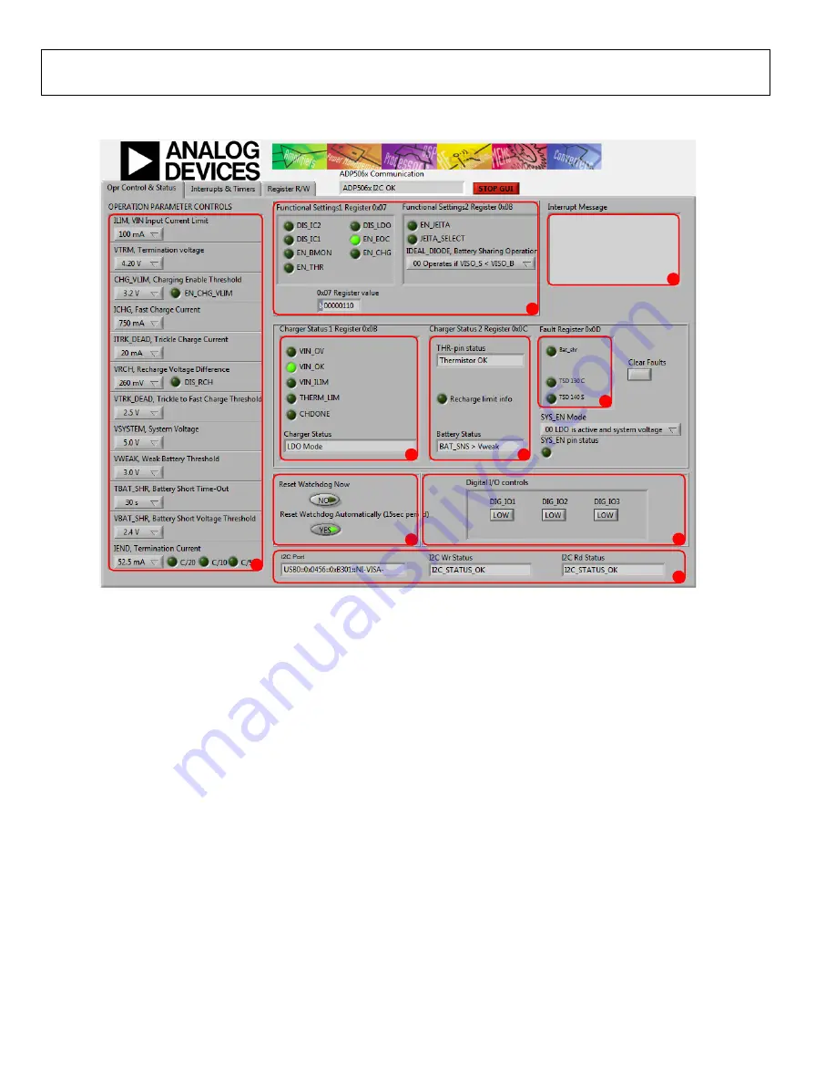
Figure 2. 

ADP5062

 GUI Operation Control and Status Tab 

The following are the GUI operation controls and status tools 
(see Figure 2): 

1.


Operation parameter controls 

2.


Functional enables 

3.


Interrupt register indicator (Register 0x0A) 

4.


Charger status 

5.


Battery status 

6.


Fault indicators 

7.


Watchdog control 

8.


Digital I/O controls 

9.


I

2

C Communication Status Indicators 

OPERATING THE BOARD WITH THE GUI 

Complete the following steps to use the board: 

1.


Before running the software, ensure that the Analog Devices 
USB-SDP-CABLEZ to the USB port of the PC.  

2.


Connect a 5 V power supply to VIN_F. 

3.


Click 

START

 > 

All Programs

 > 

ADP506x GUI

 3Vx SDP> 

ADP506x GUI SDP

. Once this step is done, the software is 

ready to use. 

VIN must be above 2.5 V in order for the I

2

C communication of 

the

 ADP5062

 to start working. The VIN voltage level is monitored, 

and the indicators are shown in the charger status indicators 

(see Number 4 in Figure 2). The GUI automatically reads the 
content of the registers after every 0.3 seconds from the last 
action and updates the status of the registers on screen. 

If there is a problem in the I

2

C communication, the status 

indicators will show an error message (see Number 9 in Figure 2). 
When I

2

C communication is operational, status indicators show 

I2C_STATUS_OK (see Figure 2). 

BASIC CHARGING PARAMETER SETTINGS 

After the input power supply is connected and is between 4.0 V 
and 6.7 V, the 

ADP5062

 is operational and capable of charging 

the battery. Charging starts with default operational parameter 
settings. It is possible to change settings using the controls on 
the left side of the 

Opr Control & Status 

tab. 


Summary of Contents for ADP5062

Page 1: ...g Devices Inc SOFTWARE REQUIREMENTS Analog Devices ADP5062 SDP evaluation software GENERAL DESCRIPTION The ADP5062 charger evaluation system is composed of an evaluation board an USB A to USB micro B...

Page 2: ...the Software Graphical User Interface GUI 4 Operating the Board with the GUI 4 Basic Charging Parameter Settings 4 Setting Interrupts 5 Setting Timers 5 Direct Register Read and Write 6 Evaluation Boa...

Page 3: ...uation software the drivers for the USB SDP CABLEZ must be installed The software and the instructions can be obtained from www analog com usb sdp cablez After proper installation of the USB SDP CABLE...

Page 4: ...UI SDP Once this step is done the software is ready to use VIN must be above 2 5 V in order for the I2 C communication of the ADP5062 to start working The VIN voltage level is monitored and the indica...

Page 5: ...automatically read after every 0 3 second timeout from the last user action involving the GUI When a certain interrupt is enabled and there is a status change in the corresponding function during char...

Page 6: ...ontents of each register in the GUI A single register read or write can be done using the controls on the right side of the Register R W tab of the GUI Type the I2 C sub address in the Sub Address for...

Page 7: ...variable power resistor or electronic load for the ISO_S_x pins The SMU at the ISO_B node must have a 100 m to 250 m resistor RS in series with its positive lead The resistor emulates the equivalent s...

Page 8: ...e the higher end of the input current limit programming range TRICKLE CHARGE CURRENT Trickle charge can only be activated during a battery charging startup sequence if the voltage level at the ISO_Bx...

Page 9: ...ge to 5 0 V 2 Set the termination voltage to 4 2 V using the GUI 3 Disable the EOC by setting the EN_EOC bit D2 to low in the functional settings register Register 0x07 4 Disable charge complete timer...

Page 10: ...et VISO_B to 3 9 V 3 Set the charge current setting to 750 mA using the GUI 4 Set VIN input current limit to 1500 mA 5 Enable charging EN_CHG high 6 Measure current to ISO_Bx value should be 750 mA 7...

Page 11: ...uF TP11 1 SN3 JP3 HeaderLarge10x2 1 2 3 4 5 6 7 8 9 10 11 12 13 14 15 16 17 18 19 20 R16 0R TP20 1 C2 1u R5 N A C6 100n TP13 1 R1 56k TP9 1 R11 0R ISO_B_S ISO_B_F SYS_EN BAT_SNS SDA ISO_S_S SCL AGND A...

Page 12: ...tor headers 3 pins 1 pin Sullins Electronics PEC36SAAN 6 J5 J6 J7 J8 J9 J10 Connector headers 2 pins 1 pin Sullins Electronics PEC36SAAN 1 R1 Resistor 56 k 1 0805 SMD Vishay or equivalent CRCW080556K0...

Page 13: ...Evaluation Board User Guide UG 500 Rev 0 Page 13 of 15 NOTES...

Page 14: ...UG 500 Evaluation Board User Guide Rev 0 Page 14 of 15 NOTES...

Page 15: ...party for any reason Upon discontinuation of use of the Evaluation Board or termination of this Agreement Customer agrees to promptly return the Evaluation Board to ADI ADDITIONAL RESTRICTIONS Custome...

Reviews: