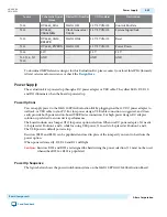
Source
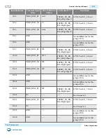
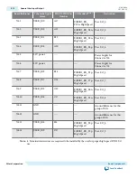
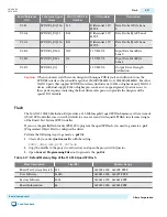
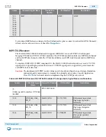
Schematic Signal Name
Device/Pin
Number
I/O Standard
Description
J1.3,
J1.4,
J1.8,
J1.15,
J1.18,
J1.21,
J1.24,
J1.27,
J1.30,
J1.31
GND
GND
GND
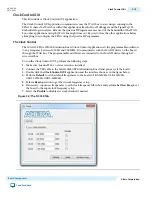
To download MIPI reference designs for this Evaluation Kit, please contact your local Intel PSG (formerly
Altera) sales team for assistance or check the
DesignStore
.
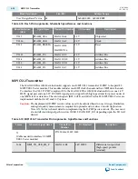
MIPI CSI-2 Receiver
The MAX 10 FPGA 10M50 Evaluation Kit supports MIPI CSI-2 receiver D-PHY to both Leopard
Imaging OV10640 and UDOO OV5640 modules. The OV10640 module includes one MIPI clock channel
and four MIPI data channels, while the OV5640 module has one MIPI clock channel and two MIPI data
channels.
To interface MIPI CSI-2 D-PHY compliant I/O, the MAX 10 10M50 evaluation kit uses one 2.5V LVDS
signal pair to support high-speed mode and one 1.2V HSTL signal pair to support low-power mode for
each MIPI clock or data lane.
Caution:
The implemented D-PHY resistor values need to be adjusted based on user design. Simulation
and signal quality measurement is required for optimal resistor values. Consult Application
Note
AN-754
for technical details on implementing the D-PHY passive circuits.
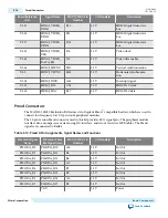
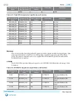
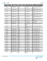
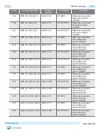
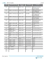
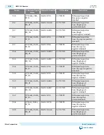
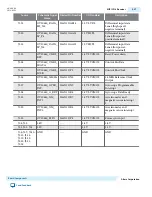
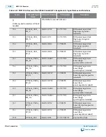
Table 3-20: MIPI CSI-2 Receiver (for OV10640 module ) Pin Assignments, Signal Names and Functions
Source
Schematic Signal
Name
Device/Pin Number
I/O Standard
Description
J2
(Cable needed to interface OV10640
module)
P/N: 52559-3652
J2.11
OV10640_CLK_
HS_P
MAX 10/P11
2.5V LVDS
Differential input clock
(high speed, positive
terminal)
J2.12
OV10640_CLK_
HS_N
MAX 10/R11
2.5V LVDS
Differential input clock
(high speed, negative
terminal)
J2.11
OV10640_CLK_
LP_P
MAX 10/T21
1.2V HSTL
Differential input clock
(low power, positive
terminal
UG-20006
2016.02.29
MIPI CSI-2 Receiver
3-25
Board Components
Altera Corporation
Send Feedback

