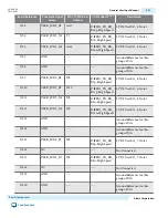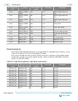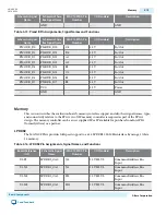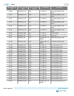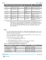
Board Reference
Type
Description
J5
USB connector
USB power supply. Use with USB Y cable
to provide 1A current. DC adapter power
and USB power don't work at the same
time.
Featured Device: MAX 10 FPGA
The MAX 10 FPGA development board features the MAX 10 10M50DAF484C6GES device (U1) in a 484-
pin FineLine BGA package.
Table 3-2: MAX 10 FPGA 10M50DAF484C6GES Features
Logic
Elements
(LEs)
Internal
Configura‐
tion
M9K
Memory
(Kb)
User Flash
Memory
(KB)
18-bit X 18-
bit
Multipliers
PLLs
ADC Blocks /
Temperature
Sensing
Diode
External Memory
Interfaces
Supported
50,000 Dual
1,638
736
Note 1
144
4
2/1
DDR3,
DDR3L,
DDR2,
LPDDR2
Note: 1. The maximum possible value including user flash memory and configuration flash memory. For
more information, refer to
MAX 10 User Flash Memory User Guide
.
Configuration
The MAX 10 10M50 Evaluation Kit supports two configuration methods:
• Configuration by downloading a .sof file to the FPGA. Any subsequent power cycling of the FPGA or
reconfiguration will power up the FPGA to a blank state.
• Programming of the on-die FPGA Configuration Flash Memory (CFM) via a .pof file. Any power
cycling of the FPGA or reconfiguration will power up the FPGA in self-configuration mode, using the
files stored in the CFM
You can use two different USB-Blaster hardware components to program the .sof or .pof files:
• Embedded USB-Blaster II, mini Type-B connector (J5)
• JTAG header (J7). Use an external USB-Blaster, USB-Blaster II, or Ethernet Blaster download cable.
The external download cable connects to the board through the JTAG header.
Using the Quartus II Programmer
You can use the Quartus II Programmer to configure the FPGA with a .sof.
Before configuring the FPGA:
• Ensure that the Quartus II Programmer and the USB-Blaster driver are installed on the host computer
• The USB cable is connected to the kit
• Power to the board is on, and no other applications that use the JTAG chain are running.
3-6
Featured Device: MAX 10 FPGA
UG-20006
2016.02.29
Altera Corporation
Board Components
Send Feedback


