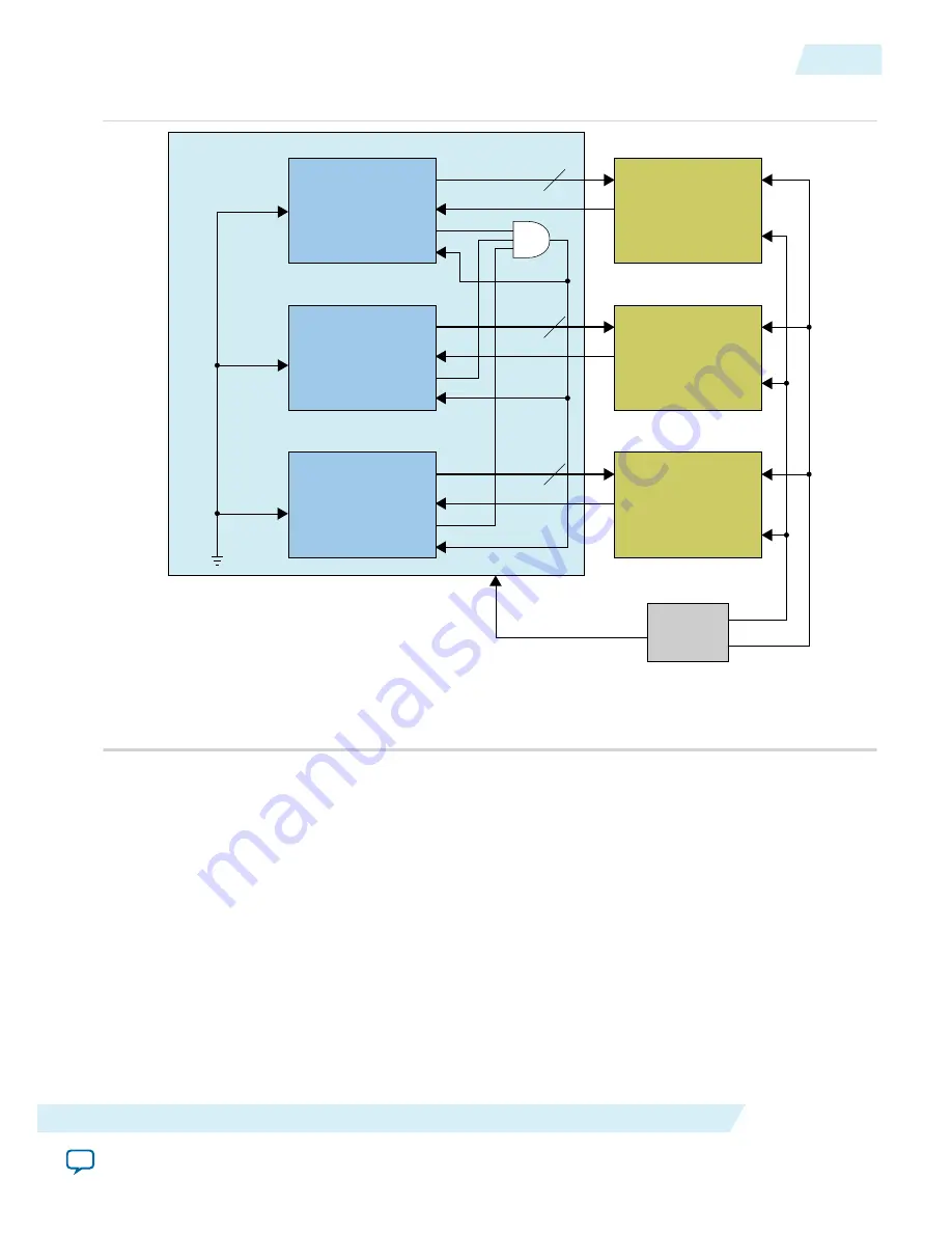
Figure 4-6: Subclass 0 — Combining the
SYNC_N
Signal for JESD204B TX IP Core
SYSREF Tied to
0 for Subclass 0
JESD204B IP Core
TX
SYSREF
SYNC_N
DEV_SYNC_N
MDEV_SYNC_N
SYSREF
SYNC_N
DEV_SYNC_N
MDEV_SYNC_N
SYSREF
SYNC_N
DEV_SYNC_N
MDEV_SYNC_N
FPGA Device
Converter Device 0
L
Converter Device 1
L
Converter Device 2
L
SYNC_N
SYNC_N
SYNC_N
Clock Chip
FPGA Reference Clock
SYNC* (1)
DAC Reference
Clock
Note:
1. SYNC* is not associated to SYNC_N in the JESD204B specification. SYNC* refers to JESD204A (Subclass 0) converter devices that
may support synchronization via additional SYNC signalling.
JESD204B IP Core
TX
JESD204B IP Core
TX
For Subclass 1 implementation, you may choose to combine or not to combine the
SYNC_N
signal from the
converter device. If you implement two ADC converter devices as a multipoint link and one of the
converter is unable to link up, the functional link will still operate. You must manage the trace length for
the
SYSREF
signal and also the differential pair to minimize skew.
The
SYNC_N
is the direct signal from the DAC converters. The error signaling from
SYNC_N
is filtered and
sent out as
dev_sync_n
output signal. The
dev_sync_n
signal from the JESD204B TX IP core must
loopback into the
mdev_sync_n
signal of the same instance without combining the
SYNC_N
signal.
Apart from that, you must set the same RBD offset value (
csr_rbd_offset
) to all the JESD204B RX IP
cores within the same multipoint link for the RBD release (the latest lane arrival for each of the links). The
JESD204 RX IP core will deskew and output the data when the RBD offset value is met. The total latency
is consistent in the system and is also the same across multiple resets. Setting a different RBD offset to
each link or setting an early release does not guarantee deterministic latency and data alignment.
UG-01142
2015.05.04
SYNC_N Signal
4-15
JESD204B IP Core Functional Description
Altera Corporation
Send Feedback


