36
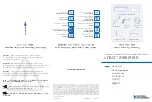
Backplane Drawing and Pin Assignments
J6 INH#: DC power inhibit signal
J8 RST#: System reset signal
J9 FAL#: Power supply fail input
J5: Connector for LED power status
J6
Pin #
Signal Name
1
INH#
2
GND
J8
Pin #
Signal Name
1
RST#
2
GND
J9
Pin #
Signal Name
1
FAL#
2
GND
J5
Name
Pin #
Pin #
Name
GND
8
7
+3.3V
GND
6
5
+5V
GND
4
3
-12V
GND
2
1
+12V
Summary of Contents for PXIS-3320
Page 4: ......
Page 12: ...4 Introduction...
Page 20: ...12 Chassis Overview...
Page 32: ...24 Specifications...
Page 34: ...26 Backplane Drawing and Pin Assignments Figure B 2 CBX 6015 rear view...