


36
•
Operation Theorem
4.5 Digital Input and Output
To program digital I/O operation is fairly straightforward. The digital input
operation is just to read data from the corresponding registers, and the digital
output operation is to write data to the corresponding registers. The digital I/O
registers
‘
format is shown in section 3.14. Note that the DIO data channel can
only be read or written in form of 16 bits together. It is impossible to access
individual bit channel.
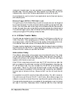
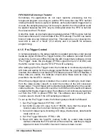
The PCI-9111 provides 16 digital input and 16 digital output channels through
the connector CN1 and CN2 on board. The digital I/O signal is fully TTL/DTL
compatible. The detailed digital I/O signal specification can be referred to
section 1.3.
Digital Output (DO)
Digital GND (DGND)
Digital Input(DI)
From TTL Signal
To TTL Devices
PCI-9111
Outside Device
74LS244
74LS373
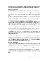
4.6 Timer/Counter Operation
4.6.1 Introduction
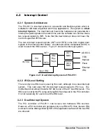
One 8254 programmable interval timer/counter chip is installed on PCI-9111.
There are three counters in one 8254 chip and 6 possible operation modes for
each counter. The block diagram of the timer/counter system is shown in
following diagram.
Counter #0
Internal 2 MHz Clock
Timer #1
Internal Timer Pacer
Timer #2
8254 Chip
G
C
G
C
G
O
O
O
'H'
'H'
AD Trigger Signal
Gate Control
Pre-Trigger
Control
Pre-Trigger
Signal
(Pin -12 of CN3)
C
Figure 4.6.1 Timer/Counter System of PCI-9111
Summary of Contents for NuDAQ PCI-9111DG
Page 1: ...NuDAQ PCI 9111DG HR Multi Functions Data Acquisition Card User s Guide ...
Page 4: ......
Page 10: ......


