


Registers Format
•
15
Please do not try to modify the base address and interrupt which assigned by
the PCI PnP BIOS, it may cause resource confliction in your system.
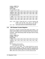
3.2 I/O Address Map
Most of the PCI-9111 registers are 16 bits. The users can access these
registers by 16 bits I/O instructions. The following table shows the
registers map, including descriptions and their offset addresses relative to
the base address.
I/O Address
Write
Read
Base + 00h
DA value
AD FIFO value
Base + 02h
Digital Output
Digital Input
Base + 04h
Extended DO
Extended DI
Base + 06h
AD channel control
AD channel read back
Base + 08h
AD range control
AD range and AD status
read back
Base + 0Ah
AD trigger mode
AD mode and interrupt
setting read back
Base + 0Ch
Interrupt control
(Not used)
Base + 0Eh
Software AD trigger
(Not used)
Base + 10h ~3Eh
Reserved
Base + 40h
Timer 8254 Ch#0
Base + 42h
Timer 8254 Ch#1
Base + 44h
Timer 8254 Ch#2
Base + 46h
Timer Control
Timer Status
Base + 48h
Clear H/W IRQ
(Not used)
Table 3.1 I/O Address
3.3 A/D Data Registers
The PCI-9111 A/D data is stored in the FIFO after conversion. The data
can be transferred to host memory by software only. The register format
for 12 bits PCI-9111DG and 16 bits PCI-9111HR is bit-wise alignment but
not fully compatible. For 12 bits PCI-9111 data, the 4 LSBs are used to
memorize the channel number in which the AD data is stored.
Summary of Contents for NuDAQ PCI-9111DG
Page 1: ...NuDAQ PCI 9111DG HR Multi Functions Data Acquisition Card User s Guide ...
Page 4: ......
Page 10: ......


