background image

Express-SL/SLE 

69


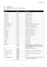
Feature  

Options  

Description  

 SECE 

Disabled 

Enabled 

Enable/Disable Root PCI Express System Error on 
Correctable Error. 

 PME 

SCI 

Disabled 

Enabled 

Enable/Disable PCI Express PME SCI. 

 Hot 

Plug 

Disabled 

Enabled 

Enable/Disable PCI Express Hot Plug. 

               Advanced Error Reporting 

Disabled 

Enabled


Advanced Error Reporting Enable/Disable 

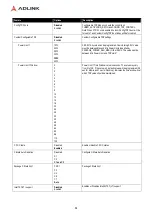
PCIe Speed 

Auto 

Gen1 
Gen2 
Gen3 

Select PCI Express port speed. 


Transmitter Half Swing 

Disabled


Enabled


Transmitter Half Swing Enable/Disable. 

Detect Non-Compiance 

Disabled 

Enabled 

Detect Non-Compliance PCI Express Device. If enabled, it 
will take more time at POST time. 

Extra Bus Reserved 

Extra Bus Reserved (0-7) for bridges behind this Root 
Bridge. 

Reseved Memory 

10 

Reserved Memory Range for this Root Bridge. 

Prefetchable Memory 

10 

Prefetchable Memory Range for this Root Bridge. 

Reserved I/O 

Reserved I/O (4K/8K/12K/16K/.../48K) Range for this Root 
Bridge. 

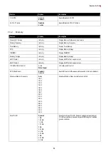
PCIE Cp 

Gen3 Equalization settings for physical PCIe lane 

PCIE Cm 

Gen3 Equalization settings for physical PCIe lane 

PCIE LTR 

Disabled 

Enabled 

PCIE Latency Reporting Enable/Disable. 

PCIE LTR Lock 

Disabled 

Enabled 

PCIE LTR Configuration Lock. 

PCIE1 CLKREQ Mapping Override 

Default 

No CLKREQ 

Custom number


PCIE CLKREQ Override for default platform mapping 

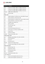
Snoop Latency Ocerrid 

Disabled 
Manual 

Auto 

Snoop Latency Ocerride for PCH PCIE. 

Non Snoop Latency Ocerrid 

Disabled 
Manual 

Auto 

Non Snoop Latency Ocerride for PCH PCIE. 


Summary of Contents for Express-SL

Page 1: ...GE COMPUTING Express SL SLE User s Manual COM Express Compact Size Type 6 Module with 6th Generation Intel Core Xeon E3 and Celeron processors Manual Rev 1 4 Revision Date July 25 2019 Part Number 50...

Page 2: ...iptions DP40 pin numbering order BIOS Select and Mode Configuration and PCI Express Configuration Switch info and BIOS menus 2018 01 23 JC 1 2 Update Intel Ethernet Controller information 2018 04 18 J...

Page 3: ...even if advised of the possibility of such damages Environmental Responsibility ADLINK is committed to fulfill its social responsibility to global environmental preservation through compliance with t...

Page 4: ...cations 12 2 12 Power Consumption 12 2 13 Operating Temperatures 12 2 14 Environmental 12 2 15 Specification Compliance 12 2 16 Operating Systems 12 2 17 Functional Diagram 13 2 18 Mechanical Dimensio...

Page 5: ...erfaces and Configuration 34 4 1 Connector Switch and LED Locations 34 4 1 1 Express SL SLE and the DB40 Module connected 34 4 2 40 pin Multipurpose Connector 35 4 3 Status LEDs 36 4 4 Fan Connector 3...

Page 6: ...and Time 56 7 3 Advanced 57 7 3 1 CPU 57 7 3 2 Memory 59 7 3 3 Graphics 60 7 3 4 SATA 63 7 3 5 USB 65 7 3 6 Network 66 7 3 7 PCI and PCIe 67 7 3 8 Super IO 71 7 3 9 ACPI and Power Management 72 7 3 1...

Page 7: ...8 2 4 PEI Beep Codes 85 8 2 5 DXE Status Codes 85 8 2 6 DXE Beep Codes 88 8 2 7 ACPI ASL Checkpoint 88 8 3 OEM Reserved Checkpoint Ranges 88 9 Mechanical Information 89 9 1 Board to Board Connectors...

Page 8: ...4 3 4 2 DirectX 11 Intel Clear Video HD Technology Advanced Scheduler 2 0 1 0 XPDM support and DirectX Video Acceleration DXVA support for full H 265 HEVC MPEG2 hardware codec Graphics outputs include...

Page 9: ...ology 2 0 Intel AVX2 Intel AES NI PCLMULQDQ Instruction Intel Device Protection Technology with Intel Secure Key Intel TSXNI Note Availability of features may vary between processor SKUs Cache 8MB for...

Page 10: ...Note Availability of features may vary between OS Win 10 8 1 7 Linux VxWorks Display Interface Support LVDS single dual channel 18 24 bit LVDS through eDP to LVDS NXP IC eDP up to 4 lane support in p...

Page 11: ...W83627DHG on carrier board 3 0x2F8 Yes 2 8 Trusted Platform Module TPM Chipset Atmel AT97SC3204 Type TPM 1 2 2 9 SEMA Board Controller Type ADLINK Smart Embedded Management Agent SEMA Supports Voltag...

Page 12: ...perating Temperatures Standard C to 60 C wide voltage input Extreme Rugged 40 C to 85 C standard voltage input 2 14 Environmental Humidity 5 90 RH operating non condensing 5 95 RH storage and operatin...

Page 13: ...Express SL SLE 13 2 17 Functional Diagram AB CD UMI...

Page 14: ...14 2 18 Mechanical Dimensions...

Page 15: ...A13 GBE0_MDI0 B13 SMB_CK C13 USB_SSRX3 D13 USB_SSTX3 A14 GBE0_CTREF B14 SMB_DAT C14 GND D14 GND A15 SUS_S3 B15 SMB_ALERT C15 DDI1_PAIR6 D15 DDI1_CTRLCLK_AUX A16 SATA0_TX B16 SATA1_TX C16 DDI1_PAIR6 D...

Page 16: ...54 GPO1 C54 TYPE0 D54 PEG_LANE_RV A55 PCIE_TX4 B55 PCIE_RX4 C55 PEG_RX1 D55 PEG_TX1 A56 PCIE_TX4 B56 PCIE_RX4 C56 PEG_RX1 D56 PEG_TX1 A57 GND B57 GPO2 C57 TYPE1 D57 TYPE2 A58 PCIE_TX3 B58 PCIE_RX3 C58...

Page 17: ...A_HSYNC C93 GND D93 GND A94 SPI_CLK B94 VGA_VSYNC C94 PEG_RX13 D94 PEG_TX13 A95 SPI_MOSI B95 VGA_I2C_CK C95 PEG_RX13 D95 PEG_TX13 A96 TPM_PP B96 VGA_I2C_DAT C96 GND D96 GND A97 TYPE10 B97 SPI_CS C97 R...

Page 18: ...ignal level I O 3 3V Bi directional signal 3 3V tolerant I O 5V Bi directional signal 5V tolerant I O 3 3Vsb Input 3 3V tolerant active in standby state P Power Input Output REF Reference voltage outp...

Page 19: ...his product Signal Pin Description I O PU PD Comment VGA_RED B89 Red for monitor Analog DAC output designed to drive a 37 5 Ohm equivalent load O Analog PD 150R shall also be terminated on the carrier...

Page 20: ...ntrol O 3 3V PD 100K LVDS_I2C_CK A83 DDC lines used for flat panel detection and control I O OD 3 3V PU 2k2 3 3V LVDS_I2C_DAT A84 DDC lines used for flat panel detection and control I O OD 3 3V PU 2k2...

Page 21: ...PHY and may be as low as 0V and as high as 3 3V The reference voltage output shall be current limited on the Module In the case in which the reference is shorted to ground the current shall be 250 mA...

Page 22: ...nel 3 Transmit Output differential pair O PCIE AC coupled on Module PCIE_RX3 PCIE_RX3 B58 B59 PCI Express channel 3 Receive Input differential pair I PCIE AC coupled off Module PCIE_TX4 PCIE_TX4 A55 A...

Page 23: ...pliant USB6 USB6 A37 A36 USB differential data pairs for Port 5 I O 3 3VSB USB 1 1 2 0 compliant USB7 USB7 B37 B37 USB differential data pairs for Port 6 I O 3 3VSB USB 1 1 2 0 compliant USB_0_1_OC B4...

Page 24: ...m module to carrier board SPI BIOS flash O 3 3VSB SPI_POWER A91 Power supply for Carrier Board SPI sourced from Module nominally 3 3V The Module shall provide a minimum of 100mA on SPI_POWER Carriers...

Page 25: ...ull down This signal is used to indicate Physical Presence to the TPM I 3 3V PD 1k PD only when TPM on module 3 3 14 SMBus Signal Pin Description I O PU PD Comment SMB_CK B13 System Management Bus bid...

Page 26: ...102 General purpose serial port receiver TTL level input I CMOS PU 47K 3 3V Power rail tolerance 5V 12V 3 3 18 Power and System Management Signal Pin Description I O PU PD Comment PWRBTN B12 Power but...

Page 27: ...SB SLEEP B103 Sleep button Low active signal used by the ACPI operating system to bring the system to sleep state or to wake it up again I OD 3 3VSB PU 10K 3 3VSB 3 3 19 Power and Ground Signal Pin De...

Page 28: ...on USB2 I PCIE AC coupled off module USB_SSTX2 USB_SSTX2 D9 D10 Additional Transmit signal differential pairs for the SuperSpeed USB data path on USB2 O PCIE AC coupled on module USB_SSRX3 USB_SSRX3 C...

Page 29: ...DI1_DDC_AUX_SEL is floating I O PCIE PD 100K DP1_AUX DDI1_CTRLCLK_AUX D15 IF DDI1_DDC_AUX_SEL pulled high I O OD 3 3V HDMI1_CTRLCLK PU 2 2K 3 3V when DDC_AUX_SEL is high IF DDI1_DDC_AUX_SEL is floatin...

Page 30: ...the DP AUX signals If pulled high the AUX pair contains the CRTLCLK and CTRLDATA signals I 3 3V PD 1M DDI 3 Signal Pin Description I O PU PD Comment DDI3_PAIR0 DDI3_PAIR0 DDI3_PAIR1 DDI3_PAIR1 DDI3_PA...

Page 31: ...2 D40 DDI2_PAIR0 DP2_LANE0 TMDS2_DATA2 D42 DDI2_PAIR1 DP2_LANE1 TMDS2_DATA1 D43 DDI2_PAIR1 DP2_LANE1 TMDS2_DATA1 D46 DDI2_PAIR2 DP2_LANE2 TMDS2_DATA0 D47 DDI2_PAIR2 DP2_LANE2 TMDS2_DATA0 D49 DDI2_PAIR...

Page 32: ...02 PCI Express Graphics transmit differential pairs I PCIE AC couple off module PEG_TX0 PEG_TX0 PEG_TX1 PEG_TX1 PEG_TX2 PEG_TX2 PEG_TX3 PEG_TX3 PEG_TX4 PEG_TX4 PEG_TX5 PEG_TX5 PEG_TX6 PEG_TX6 PEG_TX7...

Page 33: ...inatorial logic that monitors the module TYPE pins and keeps power off e g deactivates the ATX_ON signal for an ATX power supply if an incompatible module pin out type is detected The Carrier Board lo...

Page 34: ...Ds and switches that are used on the module but are not included in the standard PICMG specification 4 1 Connector Switch and LED Locations 40 pin Multi Purpose CD AB Fan 4 pin Fan BIOS Defaults Reset...

Page 35: ...ower 3 3V provide from COM module 13 BMC Program interface continued OCD0B Include a jumper to connect OCD0A via 1K0 pull up to 3 3V_BMC 32 GND 12 PWRBTN 31 BIOS_DIS0 11 SYS_RESET 30 RST 10 CB_RESET 2...

Page 36: ...Exception Codes below LED2 Green Power Source 3Vcc S0 LED ON S3 S4 S5 LED OFF ECO mode LED OFF LED3 Red BMC output and same signal as WDT B27 on BtB connector Module power up LED OFF Watchdog counting...

Page 37: ...Express SL SLE 37 4 4 Fan Connector Connector Type JVE 24W1125A 04M00 Pin Orientation 1 2 3 4 Pin Definitions Pin Signal 1 FAN_PWMOUT 2 FAN_TACHIN 3 Ground 4 5V...

Page 38: ...llowing steps 1 Shut down the system 2 Press the BIOS Setup Defaults Reset Button continuously and boot up the system You can release the button when the BIOS prompt screen appears 3 The BIOS prompt s...

Page 39: ...Express SL SLE 39 4 6 Express SL SLE Switch Settings 4 6 1 Switch Locations PCI Express Configuration Switch BIOS Select and Mode Configuration Switch...

Page 40: ...PICMG mode will configure the BIOS chips on the module as SPI0 and SPI1 In PICMG mode a BIOS chip cannot be placed in the SPI0 slot on the carrier In dual BIOS Failsafe mode both BIOS chips on the mo...

Page 41: ...CPU s PEG interface PCIe x16 The card reroutes the PCIe x16 to two x8 and allows testing of two independent PCIe add on cards with x8 x4 x2 x1 width To use the card set BIOS Advanced Graphics GFX LINK...

Page 42: ...counter counts the number of boot attempts Watchdog Timer Type II Set Reset Disable Watchdog Timer Features auto reload at power up System Restart Cause Power loss BIOS Fail Watchdog Internal Reset Ex...

Page 43: ...Current Function 5 1 2 Main Current The BMC of the Express BL implements a current monitor The current can be read by calling the SEMA function Get Main Current The function returns four 16 bit values...

Page 44: ...Exception Code Error Message 0 NOERROR 2 NO_SUSCLK 3 NO_SLP_S5 4 NO_SLP_S4 5 NO_SLP_S3 6 NO_CB_PWRGD 7 BIOS_FAIL 8 RESET_FAIL 9 RESETIN_FAIL 10 CRITICAL_TEMP 11 POWER FAIL 12 VOLTAGE_FAIL 13 NO_SYS_GD...

Page 45: ...GB 20MB 4GB 19MB 1 FEC00000 FECFFFFF 1 MB APIC Configuration Space 15MB 16MB F00000 FFFFFF 1 MB ISA Hole 1MB 15MB 100000 EFFFFF 14 MB Main Memory 0K 1MB 00000 FFFFFF 1 MB DOS Compatibility Memory 6 2...

Page 46: ...Reset Bit 0 Fast Gate A20 Bit 1 091 93 9F DMA Controller 0A0 0B1 and 0B4 0BD Interrupt controller 2 8259 equivalent 0B2 and 0B3 APM control and status port respectively 0C0 0DF DMA Controller 0E0 0EF...

Page 47: ...able 0 Counter 0 N A No 1 Keyboard controller IRQ1 via SERIRQ No 2 Cascade interrupt from slave PIC N A No 3 Serial Port 4 COM4 IRQ3 via SERIRQ PIRQ Note 1 4 Serial Port 3 COM3 IRQ4 via SERIRQ PIRQ No...

Page 48: ...Note 1 10 N A N A Note 1 11 N A N A Note 1 12 PS 2 Mouse IRQ12 via SERIRQ Note 1 13 FERR logic N A Note 1 14 SATA Primary IRQ14 via SERIRQ Note 1 15 SATA Secondary IRQ15 via SERIRQ Note 1 16 N A P E G...

Page 49: ...rnal Intel AHCI controller 00h 1Ch 00h Internal Intel PCI Express Root port 1 00h 1Ch 01h Internal Intel PCI Express Root port 2 00h 1Ch 02h Internal Intel PCI Express Root port 3 00h 1Ch 03h Internal...

Page 50: ...8 Int0 INTA 16 INTB 17 INTC 18 INTD 19 INTA 16 INTB 17 INTC 18 INTD 19 Int1 INTB 17 INTC 18 INTD 19 INTA 16 INTB 17 INTC 18 INTD 19 INTA 16 Int2 INTC 18 INTD 19 INTA 16 INTB 17 INTC 18 INTD 19 INTA 16...

Page 51: ...s are presented in bold and the function of each setting is described in the right hand column of the respective table Main Advanced Security Boot Save Exit BIOS Information Processor Information PCH...

Page 52: ...2 2 Processor Information Feature Options Description CPU Brand String Info only Display CPU Brand Name Frequency Info only Display CPU Frequency Processor ID Info only Display CPU ID Stepping Info o...

Page 53: ...Date Read only Display SMC manufacturing date Last Repair Date Read only Display SMC last repair date MAC ID Read only Display SMC MAC ID 7 2 4 2 System Management Temperatures and Fan Speed Feature...

Page 54: ...ime Statistics Info only Total Runtime Read only The returned value specifies the total time in minutes the system is running in S0 state Current Runtime Read only The returned value specifies the tim...

Page 55: ...by 0 and ends by 255 7 2 4 8 System Management Smart Fan Feature Options Description Smart Fan Info only CPU Smart FanTemperature Source CPU Sensor Board Sensor Select CPU smart fan source CPU Fan Mo...

Page 56: ...Weekday MM DD YYYY Requires the alpha numeric entry of the day of the week day of the month calendar month and all 4 digits of the year indicating the century and year Fri XX XX 20XX System Time HH MM...

Page 57: ...PU C3 state support or not CPU C6 state Info only Display CPU C6 state support or not CPU C7 state Info only Display CPU C7 state support or not L1 Data Cache Info only Display cache info L1 Code Cach...

Page 58: ...by PACKAGE_POWER_SKU_MSR Other SKUs This value must be between Min Power Limit and TDP Limit Power Limit 1 Window 0 1 2 3 4 5 6 7 8 10 12 14 16 20 24 28 32 40 48 56 64 80 96 112 128 Power Limit 1 Tim...

Page 59: ...mings XMP Profile 1 Info only Display XMP Profile 1 support or not XMP Profile 2 Info only Display XMP Profile 2 support or not I2C Write Protect Control Active Write Protect I2C write protect control...

Page 60: ...SG for Switchable Gfx Primary PEG Auto PEG1 PEG2 Select PEG0 PEG1 PEG2 PEG3 Graphics device should be Primary PEG Internal Graphics Auto Disabled Enabled Keep IGD enabled based on the setup options Ap...

Page 61: ...Active Low Vsync Polarity select Hsync Polarity Active High Active Low Hsync Polarity select LVDS eDP Backlight Mode BMC Mode GTT Mode Select LVDS Backlight control function GTT LVDS eDP Backlight Co...

Page 62: ...00 1920X1080 2048X1536 Active LFP No LVDS eDP Port A Select the Active LFP Configuration Panel Scaling Auto Off Force Scaling Select the LCD panel scaling option used by the Internal Graphics Device R...

Page 63: ...d BANNER Enabled Disabled If enabled then the OROM UI is shown Otherwise no OROM banner or information will be displayed if all disks and RAID volumes are Normal HDD Unlock Enabled Disabled If enabled...

Page 64: ...Enabled On an edge detect from 0 to 1 the PCH starts a COMRESET initialization sequence to the device SATA Device Type Hard Disk Drive Solid State Drive Identify the SATA port is connected to Solid S...

Page 65: ...B transfer time out 1 sec 5 sec 10 sec 20 sec The time out value for Control Bulk and Interrupt transfers Device reset time out 10 sec 20 sec 30 sec 40 sec USB mass storage device Start Unit command t...

Page 66: ...Confirmation Prompt MEBx Debug Message Output Enabled Disabled Enable MEBx debug message output Un Configure ME Enabled Disabled Un Configure ME without password Amt Wait Timer 0 Set timer to wait be...

Page 67: ...I Bus Clocks 160 PCI Bus Clocks 192 PCI Bus Clocks 224 PCI Bus Clocks 248 PCI Bus Clocks Value to be programmed into PCI Latency Timer Register VGA Palette Snoop Disabled Enabled Allow PCI cards that...

Page 68: ...Substates settings Gen3 Eq Phase3 Method Hardware Static Coeff Software Search PCIe Gen3 Equalization Phase 3 Method UPTP 5 Upstream Port Transmitter Preset DPTP 7 Downstream Port Transmitter Preset A...

Page 69: ...xtra Bus Reserved 0 Extra Bus Reserved 0 7 for bridges behind this Root Bridge Reseved Memory 10 Reserved Memory Range for this Root Bridge Prefetchable Memory 10 Prefetchable Memory Range for this Ro...

Page 70: ...mmed before OpROM Program Static Phase1 Eq Enabled Disable Program Phase1 Presets CTLEp Gen3 Root Port Preset Value for each lane 0 15 7 Root Port preset value per lane for Gen3 Equalization Gen3 Endp...

Page 71: ...Change Settings Enabled Disabled IO 3F8h IRQ 4 Auto IO 3F8h IRQ 4 IO 3F8h IRQ 3 4 5 6 7 9 10 11 12 IO 2F8h IRQ 3 4 5 6 7 9 10 11 12 IO 3E8h IRQ 3 4 5 6 7 9 10 11 12 IO 2E8h IRQ 3 4 5 6 7 9 10 11 12 En...

Page 72: ...rial port Select an optimal setting for Super IO device 7 3 9 ACPI and Power Management Feature Options Description ACPI and Power Management Info only Enable ACPI Auto Configuration Enabled Disabled...

Page 73: ...onsole Redirection Settings Submenu COM2 Info only Console Redirection Enabled Disabled Console Redirection Enable or Disable Console Redirection Settings Submenu COM3 Info only Console Redirection En...

Page 74: ...ANSI VT100 terminals Recorder Mode Disabled Enabled With this mode enabled only text will be sent This is to capture Terminal data Resolution 100x31 Disabled Enabled Enables or disables extended termi...

Page 75: ...alue sets the TC1 value for the ACPI Passive Cooling Formula Range 1 16 Passive TC2 Value 5 This value sets the TC2 value for the ACPI Passive Cooling Formula Range 1 16 Passive TSP Value 10 This item...

Page 76: ...uter will reboot during restart in order to change State of Security Device Device Start TPM 1 2 TPM 2 0 Auto TPM 1 2 will restrict support to TPM 1 2 devices TPM 2 0 will restrict support to TPM 2 0...

Page 77: ...Disabled Enabled Define the maximum time to wait for drive detection on PATA port SATA Support Last Boot HDD Only All SATA Devices VGA Support Auto EFI Driver If set to Auto only install Legacy OpRom...

Page 78: ...nly Legacy only Controls the execution of UEFI and Legacy Storage OpROM Video Do not launch UEFI only Legacy only Controls the execution of UEFI and Legacy Video OpROM Other PCI devices Do not launch...

Page 79: ...keys from a file with 1 Public Key Certificate in a EFI_SIGNATURE_LIST b EFI_CERT_X509 DER encoded c EFI_CERT_RSA2048 bin d EFI_CERT_SHA256 bin 2 Authenticated UEFI Variable Key Source Default Custom...

Page 80: ...ard Changes and Reset 7 6 2 Save Options Feature Options Description Save Changes Save Changes done so far to any of the setup options Discard Changes Discard Changes done so far to any of the setup o...

Page 81: ...l Platform Innovation Framework for EFI the Framework The Framework refers the following boot phases which may apply to various status code checkpoint descriptions Security SEC initial low level initi...

Page 82: ...tion 0x0 Not used Progress Codes 0x1 Power on Reset type detection soft hard 0x2 AP initialization before microcode loading 0x3 North Bridge initialization before microcode loading 0x4 South Bridge in...

Page 83: ...e module specific 0x1D 0x2A OEM pre memory initialization codes 0x2B Memory initialization Serial Presence Detect SPD data reading 0x2C Memory initialization Memory presence detection 0x2D Memory init...

Page 84: ...nstalled 0x56 Invalid CPU type or Speed 0x57 CPU mismatch 0x58 CPU self test failed or possible CPU cache error 0x59 CPU micro code is not found or micro code update is failed 0x5A Internal CPU error...

Page 85: ...arted 3 DXEIPL was not found 3 DXE Core Firmware Volume was not found 7 Reset PPI is not available 4 Recovery failed 4 S3 Resume failed 8 2 5 DXE Status Codes Status Code Description 0x60 DXE Core is...

Page 86: ...ialization South Bridge module specific 0x77 South Bridge DXE Initialization South Bridge module specific 0x78 ACPI module initialization 0x79 CSM initialization 0x7A 0x7F Reserved for future AMI DXE...

Page 87: ...s hot plug 0xB6 Clean up of NVRAM 0xB7 Configuration Reset reset of NVRAM settings 0xB8 0xBF Reserved for future AMI codes 0xC0 0xCF OEM BDS initialization codes DXE Error Codes 0xD0 CPU initializatio...

Page 88: ...is entering S5 sleep state 0x10 System is waking up from the S1 sleep state 0x20 System is waking up from the S2 sleep state 0x30 System is waking up from the S3 sleep state 0x40 System is waking up f...

Page 89: ...onnector with 0 5mm for a stacking height of 5 mm This connector can be used with 5 mm through hole standoffs SMT type Tyco 3 6318491 6 Foxconn QT002206 4141 3H 220 pin board to board connector with 0...

Page 90: ...on top of the module is compatible with all COM Express modules 9 2 2 Heat Sinks A heat sink can be used as a thermal solution for a specific COM Express module and can have a fan or be fanless depen...

Page 91: ...E uses two screws to attach the heatsink to the COM Express module Step 4 Place the COM Express module and heatsink assembly onto the connectors on the carrier board as shown Then press down on the mo...

Page 92: ...92 Step 6 If you are installing a heatsink with a fan plug the fan connector into the carrier board as shown...

Page 93: ...tion to the choice of 5 mm or 8mm board to board connectors there is the choice of Top and Bottom mounting In Top mounting the threaded standoffs are on the carrier board and the thermal solution is e...

Page 94: ...standoffs are DIP type and through hole standoffs are SMT type Other types not listed are available upon request 5mm through hole standoff SMT type P N 33 72000 0050 5mm threaded standoff DIP type P N...

Page 95: ...and warnings on the equipment should be noted Please keep this equipment from humidity Do not use this equipment near water or a heat source Lay this equipment on a reliable surface when install A dr...

Page 96: ...Toll Free 1 800 966 5200 USA only Fax 1 408 360 0222 Email info adlinktech com ADLINK Technology China Co Ltd Address 300 Fang Chun Rd Zhangjiang Hi Tech Park Pudong New Area Shanghai 201203 China Tel...

Reviews: