SERIES AP220 / AP231 ACROPACK
USER
’S MANUAL
Acromag, Inc. Tel: 248-295-0310
- 24 -
http://www.acromag.com
- 24 -
https://www.acromag.com
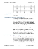
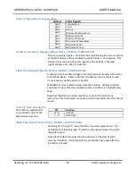
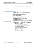
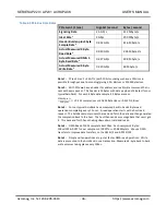
Table 3.7: System Monitor Register Map
Address
Status Register
0x00
Temperature
0x01
Vccint
0x02
Vccaux
0x20
Maximum Temperature
0x21
Maximum Vccint
0x22
Maximum Vccaux
0x24
Minimum Temperature
0x25
Minimum Vccint
0x26
Minimum Vccaux
Firmware Revision Register (Read Only) - (BAR0 + 0x0000 0200)
This is a read only register. The ASCII code representing the current revision
of the MCS firmware file is readable from this location. For example, if the
firmware is at revision A then this register will read 0x41 in the least
significant byte or B= 0x42, C=0x43, etc.
Flash Data Register (Read/Write) - (BAR0 + 0x0000 0204)
A byte write to this address triggers a write/read serial transfer to/from the
serial FLASH device. A byte read from this address returns the data read
from a previous write/read serial transfer.
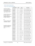
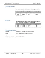
WARNING: Factory calibration data is stored in FLASH. Writing to FLASH
could result in loss of factory calibration data. See Table 3.7 Flash Memory
Map.
Note that the Flash chip select must be set prior to the start of any
instruction. Flash chip select must also be driven high after the instruction is
issued.
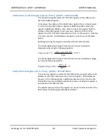
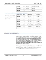
Table 3.8 Flash Data Register
Note that any registers/bits
not used will remain at the
default value logic low.
BIT
Function
31 - 8
Unused
7 - 0
Flash Data
Flash Chip Select (Write Only) - (BAR0 + 0x0000 0208)
Asserting bit-
0 to logic “0” drive the Flash chip select signal active. The
default state of this bit is logic “1” which is the inactive state of
the Flash
chip select signal.
Note that the Flash chip select must be set prior to the start of Flash
memory instruction. Flash chip select must also be driven high after the
instruction is issued.

