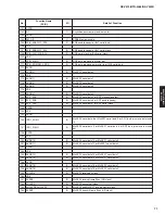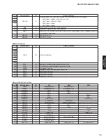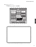
Control Pins
Configuration Pins
CEC Pins
Pin
No.
Function Name
Type
I/O
Detail of Function
Local configuration/status I2C clock.
66
CSCL
Schmitt Open drain 5
V tolerant
Input
Chip configuration/status is accessed via this I2C port. This pin is true open
drain, so it does not pull to ground if power is not applied.
Local configuration/status I2C data.
67
CSDA
LVTTL Schmitt Open
drain 5 V tolerant
Input/Output
Chip configuration/status is accessed via this I2C port. This pin is true open
drain, so it does not pull to ground if power is not applied.
External reset.
Active LOW. Must be pulled up to VCC33OUT. When main power is not provided
to the system, the microprocessor must present a high impedance of at least
100 k-ohms to RESET#. If this condition is not met, a circuit to block the leakage
from VCC33OUT to the microprocessor GPIO may be required.
69
RESET#
Schmitt
Input
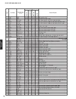
Pin
No.
Function Name
Type
I/O
Detail of Function
I2C slave address input / Transmit power sense output.
During power-on-reset (POR), this pin is used as an input to latch the I2C
subaddress. The level on this pin is latched when the POR transitions from the
asserted state to the de-asserted state.
70
TPWR_CI2CA
LVTTL
Input/Output
After completion of POR, this pin is used as the TPWR output. A register setting
can change this pin to show if the active port is receiving a TMDS clock.
68
INT
Schmitt Open drain
8 mA 3.3 V tolerant
Output
Interrupt output.
This is an open-drain output and requires an external pull-up resistor.
Pin
No.
Function Name
Type
I/O
Detail of Function
Primary CEC I/O used for interfacing to CEC devices This signal is electrically
compliant with the CEC specification.
As an input, this pin acts as an LVTTL schmitt triggered input and is 5 V tolerant.
As an output, the pin acts as an NMOS driver with resistive pull-up.
This pin has an internal pull-up resistor.
CEC Compliant 5V
tolerant, Schmitt
triggered, LVTTL
This signal should be connected to the CEC signal of all HDMI input and output
ports if the system supports just one CEC line.
72
CEC_A0
Input/Output
OR
In a system designed to have separate CEC connectivity for the HDMI input and
output ports, this signal should be connected to the CEC signal of all the input
ports supported in the system.
This signal and CEC_A0 each connect to a separate CEC controller within the
port processor and are independent of each other.
Secondary CEC I/O used for interfacing to CEC devices.
This signal is electrically compliant with the CEC specification. As an input, this
pin acts as an LVTTL schmitt triggered input and is 5 V tolerant. As an output,
the pin acts as an NMOS driver with resistive pull-up. This pin has an internal
pull-up resistor.
CEC Compliant 5V
tolerant, Schmitt
triggered, LVTTL
This is an optional CEC signal provided for system designers who want to
implement a system with two independent CEC lines, such as a system that
supports a separate CEC line for the HDMI input ports and the HDMI output
ports. In the example of a DTV that provides a second HDMI output using the
SiI957n port processor; this signal can be connected to the CEC signal of the
output port while the CEC_A1 signal is connected to the CEC signal of the input
ports.
71
CEC_A1
Input/Output
This signal and CEC_A1 each connect to a separate CEC controller within the
port processor and are independent of each other.
66
RX-V475/HTR-4066/RX-V500D
RX-V475/HTR-4066/
RX-V50
0D
Содержание RX-V500D
Страница 9: ...RX V500D A model RX V500D B G models 9 RX V475 HTR 4066 RX V500D RX V475 HTR 4066 RX V500D ...
Страница 132: ... CONFIGURING THE SYSTEM SETTINGS RX V475 HTR 4066 RX V500D 133 ...
Страница 133: ... システム設定を変更する RX V475 HTR 4066 RX V500D 134 ...
Страница 146: ...147 RX V475 HTR 4066 RX V500D RX V475 HTR 4066 RX V500D MEMO ...
Страница 147: ...RX V475 HTR 4066 RX V500D ...

