background image

7

Circuit Description

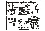
Reception and transmission are switched by “RX” and
“TX” lines from the microprocessor unit (MPU). The re-
ceiver uses double-conversion superheterodyne circuitry,
with a 21.7 MHz 1st IF and 450 kHz 2nd IF. The 1st lo-
cal, produced by a PLL synthesizer, yields the 21.7 MHz
1st IF.

The 2nd local uses a 21.250 MHz (21.7 MHz - 450 kHz)
signal generated by a crystal oscillator. The 2nd mixer
and other circuits use a custom IC to convert and amplify
the 2nd IF, and detect FM to obtain demodulated signals.

During transmit, the PLL synthesizer oscillates at the de-
sired frequency directly, for amplification to obtain RF
power output. During transmit, voice modulation and
CTCSS (or DCS) modulation are applied to this synthe-
sizer. Transceiver functions, such as TX/RX control, PLL
synthesizer settings, and channel programming, are con-
trolled using the MPU.

Receiver

Incoming RF signals from the antenna connector are de-
livered to the RF Unit, and pass through a lowpass filter
(LPF) consisting of coils L303, L305, and L307, capaci-
tors C303, C309, C310, and C316, and antenna switching
diodes 

D305

 and 

D306

 (Both 

MA111

) for delivery to the

receiver front end.

Signals within the frequency range of the transceiver are
then passed through a varactor-tuned bandpass filter con-
sisting of diodes 

D308

D322

D310

 and 

D323

 (all

HVC3508

), and coils L334, L335, L320 and L322 and

associated circuitry before RF amplification by 

Q316

(

3SK240

).

The amplified RF signal is then bandpass filtered again
by varactor-tuned resonators consisting of diodes 

D312

,

D324

D313

 and 

D325

 (all 

HVC3508

), and coils L336,

L337, L325 and L327 and associated circuitry, to ensure
pure in-band input to 1st mixer 

Q321

 (

3SK240

).

Buffered output from the VCO Unit is amplified by 

Q318

(

2SC5006

) and lowpass-filtered by L339, C414, and

C413, to provide a pure 1st local signal between 112.3
and 152.3 MHz, which is delivered to the 1st mixer.

The 21.7 MHz 1st mixer product then passes through dual
monolithic crystal filter F301 (7.5 kHz BW), and is am-
plified by 

Q327

 (

2SC4215Y

) and delivered to the input

of the FM IF subsystem IC 

Q334

 (

TA31136FN

).

This IC contains the 2nd mixer, 2nd local oscillator, lim-
iter amplifier, FM detector, noise amplifier, S-meter am-
plifier and squelch gates.

The 2nd local in the IF-IC is produced from crystal 

X302

(21.250 MHz), and the 1st IF is converted to 450 kHz by
the 2nd mixer and stripped of unwanted components by
ceramic filter 

F302

. After passing through a limiter am-

plifier, the signal is demodulated by the FM detector.

Demodulated receive audio from the IF-IC is amplified
by 

Q336

 (

2SA1588Y

) and 

Q338

 (

UMX2M

). After vol-

ume adjustment by the AF power amplifier 

Q337

(

LA4425A

), the audio signal is passed to the optional

headphone or 8-ohm loudspeaker.

PLL Synthesizer

The 1st local maintains stability from the PLL synthesiz-
er by using a 21.250 MHz reference signal from crystal

X301

. PLL synthesizer IC 

Q333

 (

LV2105V

) consists of

a prescaler, reference counter, swallow counter, program-
mable counter, a serial data input port to set these counters
based on external data, a phase comparator, and a charge
pump.

The PLL-IC divides the 21.250 MHz reference signal by
4,250 using the reference counter (5.0 kHz comparison
frequency). The VCO output is divided by the prescaler,
swallow counter and programmable counter. These two
signals are compared by the phase comparator and ap-
plied to the charge pump. A voltage proportional to their
phase difference is delivered to the low-pass filter circuit,
then fed back to the VCO as a voltage with phase error,
controlling and stabilizing the oscillating frequency. This
synthesizer also operates as a modulator during transmit.

The RX VCO is comprised of 

Q323

 (

2SC5006

) and

D314

/

D326

 (Both 

1SV282

), and oscillates at 21.7 MHz

during receive.

The TX VCO is comprised of 

Q322

 (

2SC5006

) and

D316

/

D327

 (Both 

1SV282

) and oscillates at the funda-

mental frequency during transmit, with direct frequency-
modulation using varactor diode 

D315

 (

1SV214

).

The VCO output passes through buffer amplifier 

Q320

(

2SC5005

), and a portion is fed to the PLL IC, and at the

same time is amplified by 

Q318

 (

2SC5006

) to obtain

stable output. Synthesizer output is fed to the 1st mixer
by diode switch 

D311

 (

1SS321

) during receive,  and to

pri-drive amplifier 

Q317

 (

2SC3356

) for transmit.

The reference oscillator feeds the PLL synthesizer, and is
composed of crystal 

X301

 (21.250 MHz) and transmit

(DCS) modulation circuit 

D317

 (

HVC350B

).

The VCO DC supply is regulated by 

Q330

 (

2SC4617

).

Содержание FT-2800M

Страница 1: ...occur as a result of typographical or other errors that may be present Your cooperation in pointing out any inconsistencies in the technical information would be appreciated 2007 VERTEX STANDARD CO LT...

Страница 2: ...ure Range 4 F to 140 F 20 C to 60 C Case Size WxHxD 6 3 x 2 0 x 7 3 160 x 50 x 185 mm w o knobs Weight Approx 4 0 lb 1 8 kg Transmitter Output Power 65 W 25 W 10 W 5 W Modulation Type Variable Reactan...

Страница 3: ...M ASSY S8002052 KNOB VOL S8002053 KNOB DIAL S8002052 KNOB VOL S8101433 SPEAKER S8101435 CABLE with BLADE FUSE S8002064 SPACER S8002055 PLATE EARTH S8002057 CASE MAIN S8002056 REFLECTOR COM Unit S80020...

Страница 4: ...4 Exploded View Miscellaneous Parts Note...

Страница 5: ...Block Diagram...

Страница 6: ...Block Diagram Note...

Страница 7: ...2nd local oscillator lim iter amplifier FM detector noise amplifier S meter am plifier and squelch gates The 2nd local in the IF IC is produced from crystal X302 21 250 MHz and the 1st IF is converted...

Страница 8: ...313 2SK3075 and power amplifier Q305 RD70HVS1 to obtain full RF output The RF energy then passes through antenna switch D303 XB15A407 and a low pass filter circuit and finally to the antenna connector...

Страница 9: ...ent and thorough familiarity with its correct use is necessary for complete realign ment Correction of problems caused by misalignment resulting from use of improper test equipment is not cov ered und...

Страница 10: ...save the new setting 5 Press and hold the MHz key for one second to exit to the normal operation PLL VCO 1 Connect the DC voltmeter to TP RVC on the RF Unit 2 Tune the frequency to 146 000 MHz 3 Adju...

Страница 11: ...from the RF Signal Generator 3 Press and hold the LOW key for one second to save the new setting 4 Rotate the DIAL knob one click to clockwise to set the Alignment parameter to SMTL 2 5 Reduce the RF...

Страница 12: ...E W TONE N 1 Tune the transceiver to 146 000 MHz 2 Set the CTCSS tone to 100 Hz Press and hold the MHz key for one second to activate the Set Menu mode Rotate the DIAL knob to select 27 SQ TNF Press t...

Страница 13: ...COM Unit RF Unit Circuit Diagram...

Страница 14: ...COM Unit RF Unit Circuit Diagram Note...

Страница 15: ...B 2SJ144Y VY Q101 107 135 NJM2902V Q102 DTC144EU 26 Q103 104 130 136 137 NJM2904V Q105 BU4094BCFV Q106 109 2SC4617R BR Q110 111 115 130 132 CAT24WC64JI Q112 1SS302 C3 D101 102 116 118 DAP202U P D104...

Страница 16: ...TB Q113 R114 C114 C119 C132 R167 R146 R192 R191 R184 R189 R183 R182 C151 C150 R180 Q109 Q106 Q112 Q105 Q102 Q115 Q116 X101 R148 Q135 R201 C155 C161 R209 R151 R139 R136 R137 R138 L104 L106 C124 C122 C1...

Страница 17: ...a b c d e f g 1 2 Side A Side B 2SJ144Y VY Q101 107 135 NJM2902V Q102 DTC144EU 26 Q103 104 130 136 137 NJM2904V Q105 BU4094BCFV Q106 109 2SC4617R BR Q110 111 115 130 132 CAT24WC64JI Q112 1SS302 C3 D1...

Страница 18: ...18 Note...

Страница 19: ...1 C 131 CHIP CAP 1uF 10V B GRM188B11A105KA61D S8101390 1 C 132 CHIP CAP 1uF 10V B GRM188B11A105KA61D S8101390 1 C 133 CHIP CAP 0 001uF 50V B GRM188B11H102KA01D K22174821 1 C 134 AL ELECTRO CAP 100uF...

Страница 20: ...C 4 7uH LK1608 4R7K T L1690688 1 L 105 M RFC 4 7uH LK1608 4R7K T L1690688 1 L 106 M RFC 4 7uH LK1608 4R7K T L1690688 1 Q 101 FET 2SJ144Y TE85R F G3701447Y 1 Q 102 IC NJM2902V TE1 G1091679 1 Q 103 TRAN...

Страница 21: ...IP RES 47k 1 16W 5 RMC1 16 473JATP J24185473 TYPE A1 19 R 151 CHIP RES 47k 1 16W 5 RMC1 16 473JATP J24185473 TYPE A2 19 R 151 CHIP RES 220k 1 16W 5 RMC1 16 224JATP J24185224 TYPE A3 19 R 151 CHIP RES...

Страница 22: ...HIP RES 3 3k 1 16W 5 RMC1 16 332JATP J24185332 47 R 212 CHIP RES 0 1 16W 5 RMC1 16 000JATP J24185000 1 R 220 CHIP RES 100k 1 16W 5 RMC1 16 104JATP J24185104 1 R 221 CHIP RES 390k 1 16W 5 RMC1 16 394JA...

Страница 23: ...23 A B C D E F G 1 2 3 4 5 Side A RD70HVF1 Q306 2SB1197K AH Q303 307 DTC144EU 26 Q304 324 DTA114EU 14 Q325 326 2SC5006 24 Q320 322 323 RF Unit Parts Layout Lot 1 15...

Страница 24: ...24 a b c d e f g 1 2 3 4 5 Side B 1SS312 D302 311 RF Unit Parts Layout Lot 1 15...

Страница 25: ...D307 C351 Q306 C378 C372 C372 R333 C366 C315 C333 L308 C535 R440 X302 C424 F302 F301 D308 C427 D315 C443 R391 R390 C440 L318 L340 C534 R383 C430 R389 R396 R375 C538 R398 C340 D305 C343 R377 C374 R470...

Страница 26: ...57 C507 C498 C503 C501 C506 R458 C511 Q333 Q334 R342 L322 C392 R330 C312 R303 C308 R479 R305 L320 D302 D329 R482 C451 C449 C448 Q331 R417 C502 C499 C508 C510 C329 C339 L332 Q310 Q317 Q328 Q315 C359 C3...

Страница 27: ...27 A B C D E F G 1 2 3 4 5 Side A RD70HVF1 Q306 2SB1197K AH Q303 307 DTC144EU 26 Q304 324 DTA114EU 14 Q325 326 2SC5006 24 Q320 322 323 RF Unit Parts Layout Lot 57...

Страница 28: ...28 a b c d e f g 1 2 3 4 5 Side B 1SS312 D302 311 RF Unit Parts Layout Lot 57...

Страница 29: ...92 1 C 336 CHIP CAP 0 001uF 50V B GRM188B11H102KA01D K22174821 1 C 337 CHIP CAP 0 001uF 50V B GRM188B11H102KA01D K22174821 1 C 338 CHIP CAP 0 001uF 50V B GRM188B11H102KA01D K22174821 1 C 339 CHIP CAP...

Страница 30: ...CAP 0 001uF 50V B GRM188B11H102KA01D K22174821 1 C 408 CHIP CAP 0 001uF 50V B GRM188B11H102KA01D K22174821 1 C 409 AL ELECTRO CAP EMV 250ADA4R7MB55G S8101397 1 C 410 CHIP CAP 100pF 50V CH GRM1882C1H10...

Страница 31: ...1 C 483 CHIP CAP 0 01uF 50V B GRM188B11H103KA01D K22174823 1 C 484 CHIP CAP 0 01uF 50V B GRM188B11H103JA01D K22174824 TYPE B3 19 C 485 CHIP CAP 0 001uF 50V B GRM188B11H102KA01D K22174821 1 C 486 CHIP...

Страница 32: ...188B11H103KA01D K22174823 50 C 563 CHIP CAP 10pF 50V CH GRM1882C1H100JA01D K22174211 51 C 564 CERAMIC CAP 0 001uF 50V B UP050B102K A B K28179001 70 D 301 SURGE ABSORBER P6KE18A Q9000630 1 D 302 DIODE...

Страница 33: ...7uH LK1608 4R7K T L1690688 1 L 342 INDUCTOR MLF1608DR22KT S8101412 1 L 343 M RFC 0 0056uH LL1608 FSL5N6S L1690858 TYPE B1 19 L 343 M RFC 0 0056uH LL1608 FSL5N6S L1690858 TYPE B2 19 Q 301 TRANSISTOR 2S...

Страница 34: ...5 RMC1 16 471JATP J24185471 1 R 335 CHIP RES 5 6k 1 16W 5 RMC1 16 562JATP J24185562 1 R 336 CHIP RES 220 1 16W 5 RMC1 16 221JATP J24185221 1 R 337 CHIP RES 4 7k 1 16W 5 RMC1 16 472JATP J24185472 1 R 3...

Страница 35: ...47k 1 16W 5 RMC1 16 473JATP J24185473 1 R 406 CHIP RES 2 7k 1 16W 5 RMC1 16 272JATP J24185272 1 R 407 CHIP RES 220k 1 16W 5 RMC1 16 224JATP J24185224 1 R 408 CHIP RES 470k 1 16W 5 RMC1 16 474JATP J24...

Страница 36: ...IP RES 22k 1 16W 5 RMC1 16 223JATP J24185223 37 R 476 CHIP RES 10k 1 16W 5 RMC1 16 103JATP J24185103 1 R 477 CHIP RES 10k 1 16W 5 RMC1 16 103JATP J24185103 1 R 479 CHIP RES 4 7k 1 16W 5 RMC1 16 472JAT...

Страница 37: ...M 1 16W 5 RMC1 16 225JATP J24185225 1 R 518 THERMISTOR TBPS1R473J475H5Q S8101388 1 R 519 CHIP RES 0 1 16W 5 RMC1 16 000JATP J24185000 1 R 520 CHIP RES 560k 1 10W 5 RMC1 10T 564J J24205564 1 R 521 CHIP...

Страница 38: ...38 REF DESCRIPTION VALUE V W TOL MFR S DESIG VXSTD P N VERS LOT SIDE LAY ADR Note...

Страница 39: ...13...

Страница 40: ...14 Copyright 2007 VERTEX STANDARD CO LTD All rights reserved No portion of this manual may be reproduced without the permission of VERTEX STANDARD CO LTD Printed in Japan...

Отзывы: