background image

9

Alignment

Introduction and Precautions

The FT-2800M has been carefully aligned at the factory
for the specified performance at the 144 MHz amateur
band. Realignment should therefore not be necessary ex-
cept in the event of a component failure. All component
replacement and service should be performed only by an
authorized Vertex Standard representative, or the warranty
policy may be voided.

The following procedures cover the sometimes critical and
tedious adjustments that are not normally required once
the transceiver has left the factory. However, if damage
occurs and some parts are replaced, realignment may be
required. If a sudden problem occurs during normal oper-
ation, it is likely due to component failure; realignment
should not be done until after the faulty component has
been replaced.

We recommend that servicing be performed only by au-
thorized Vertex Standard service technicians who are ex-
perienced with the circuitry and fully equipped for repair
and alignment. Therefore, if a fault is suspected, contact
the dealer from whom the transceiver was purchased for
instructions regarding repair. Authorized Vertex Standard
service technicians realign all circuits and make complete
performance checks to ensure compliance with factory
specifications after replacing any faulty components.

Those who do undertake any of the following alignments
are cautioned to proceed at their own risk. Problems caused
by unauthorized attempts at realignment are not covered
by the warranty policy. Also, Vertex Standard must re-
serve the right to change circuits and alignment proce-
dures in the interest of improved performance, without
notifying owners.

Under no circumstances should any alignment be attempt-
ed unless the normal function and operation of the trans-
ceiver are clearly understood, the cause of the malfunc-
tion has been clearly pinpointed and any faulty compo-
nents replaced, and the need for realignment determined
to be absolutely necessary.

Required Test Equipment

The following test equipment (and thorough familiarity
with its correct use) is necessary for complete realign-
ment. Correction of problems caused by misalignment
resulting from use of improper test equipment is not cov-
ered under the warranty policy. While most steps do not
require all of the equipment listed, the interactions of some
adjustments may require that more complex adjustments
be performed afterwards. Do not attempt to perform only
a single step unless it is clearly isolated electrically from
all other steps. Have all test equipment ready before be-
ginning, and follow all of the steps in a section in the
order presented.

ˆ

Regulated DC Power Supply: adjustable from 10 to 17
VDC, 15 A

ˆ

RF Signal Generator with calibrated output level at
200 MHz

ˆ

Frequency Counter: ±0.1 ppm accuracy at 200 MHz

ˆ

AF Signal Generator

ˆ

SINAD Meter

ˆ

Deviation Meter (linear detector)

ˆ

AF Milivoltmeter

ˆ

AF Dummy Load: 8-Ohm, 5 W

ˆ

DC Voltmeter: high impedance

ˆ

Inline Wattmeter with 5% accuracy at 200 MHz

ˆ

50-Ohm non-reactive Dummy Load:

ˆ

100 watts at 200 MHz

ˆ

VHF Sampling Coupler

Set up the test equipment as shown for the transceiver
alignment, and apply 13.8 VDC power to the transceiver.

Alignment Preparation & Precautions

A dummy load and inline wattmeter must be connected to
the antenna jack in all procedures that call for transmis-
sion, except where specified otherwise. Correct alignment
is not possible with an antenna. After completing one step,
read the following step to determine whether the same
test equipment will be required. If not, remove the test
equipment (except dummy load and wattmeter, if connect-
ed) before proceeding.

Correct alignment requires that the ambient temperature
in the repair shop be the same as that of the transceiver
and test equipment, and that this temperature be held con-
stant between 68 °C and 86 °F (20 °C ~ 30 °C). When the
transceiver is brought into the shop from hot or cold air it
should be allowed some time for thermal equalization with
the environment before alignment. If possible, alignments
should be made with oscillator shields and circuit boards
firmly affixed in place. Also, the test equipment must be
thoroughly warmed up before beginning.

Notes

: Signal levels in dB referred to in alignment are

based on 0 dB

μ

 = 0.5 

μ

V.

Содержание FT-2800M

Страница 1: ...occur as a result of typographical or other errors that may be present Your cooperation in pointing out any inconsistencies in the technical information would be appreciated 2007 VERTEX STANDARD CO LT...

Страница 2: ...ure Range 4 F to 140 F 20 C to 60 C Case Size WxHxD 6 3 x 2 0 x 7 3 160 x 50 x 185 mm w o knobs Weight Approx 4 0 lb 1 8 kg Transmitter Output Power 65 W 25 W 10 W 5 W Modulation Type Variable Reactan...

Страница 3: ...M ASSY S8002052 KNOB VOL S8002053 KNOB DIAL S8002052 KNOB VOL S8101433 SPEAKER S8101435 CABLE with BLADE FUSE S8002064 SPACER S8002055 PLATE EARTH S8002057 CASE MAIN S8002056 REFLECTOR COM Unit S80020...

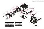
Страница 4: ...4 Exploded View Miscellaneous Parts Note...

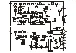
Страница 5: ...Block Diagram...

Страница 6: ...Block Diagram Note...

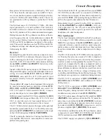
Страница 7: ...2nd local oscillator lim iter amplifier FM detector noise amplifier S meter am plifier and squelch gates The 2nd local in the IF IC is produced from crystal X302 21 250 MHz and the 1st IF is converted...

Страница 8: ...313 2SK3075 and power amplifier Q305 RD70HVS1 to obtain full RF output The RF energy then passes through antenna switch D303 XB15A407 and a low pass filter circuit and finally to the antenna connector...

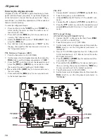
Страница 9: ...ent and thorough familiarity with its correct use is necessary for complete realign ment Correction of problems caused by misalignment resulting from use of improper test equipment is not cov ered und...

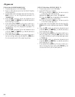
Страница 10: ...save the new setting 5 Press and hold the MHz key for one second to exit to the normal operation PLL VCO 1 Connect the DC voltmeter to TP RVC on the RF Unit 2 Tune the frequency to 146 000 MHz 3 Adju...

Страница 11: ...from the RF Signal Generator 3 Press and hold the LOW key for one second to save the new setting 4 Rotate the DIAL knob one click to clockwise to set the Alignment parameter to SMTL 2 5 Reduce the RF...

Страница 12: ...E W TONE N 1 Tune the transceiver to 146 000 MHz 2 Set the CTCSS tone to 100 Hz Press and hold the MHz key for one second to activate the Set Menu mode Rotate the DIAL knob to select 27 SQ TNF Press t...

Страница 13: ...COM Unit RF Unit Circuit Diagram...

Страница 14: ...COM Unit RF Unit Circuit Diagram Note...

Страница 15: ...B 2SJ144Y VY Q101 107 135 NJM2902V Q102 DTC144EU 26 Q103 104 130 136 137 NJM2904V Q105 BU4094BCFV Q106 109 2SC4617R BR Q110 111 115 130 132 CAT24WC64JI Q112 1SS302 C3 D101 102 116 118 DAP202U P D104...

Страница 16: ...TB Q113 R114 C114 C119 C132 R167 R146 R192 R191 R184 R189 R183 R182 C151 C150 R180 Q109 Q106 Q112 Q105 Q102 Q115 Q116 X101 R148 Q135 R201 C155 C161 R209 R151 R139 R136 R137 R138 L104 L106 C124 C122 C1...

Страница 17: ...a b c d e f g 1 2 Side A Side B 2SJ144Y VY Q101 107 135 NJM2902V Q102 DTC144EU 26 Q103 104 130 136 137 NJM2904V Q105 BU4094BCFV Q106 109 2SC4617R BR Q110 111 115 130 132 CAT24WC64JI Q112 1SS302 C3 D1...

Страница 18: ...18 Note...

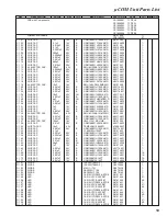
Страница 19: ...1 C 131 CHIP CAP 1uF 10V B GRM188B11A105KA61D S8101390 1 C 132 CHIP CAP 1uF 10V B GRM188B11A105KA61D S8101390 1 C 133 CHIP CAP 0 001uF 50V B GRM188B11H102KA01D K22174821 1 C 134 AL ELECTRO CAP 100uF...

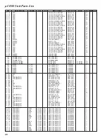
Страница 20: ...C 4 7uH LK1608 4R7K T L1690688 1 L 105 M RFC 4 7uH LK1608 4R7K T L1690688 1 L 106 M RFC 4 7uH LK1608 4R7K T L1690688 1 Q 101 FET 2SJ144Y TE85R F G3701447Y 1 Q 102 IC NJM2902V TE1 G1091679 1 Q 103 TRAN...

Страница 21: ...IP RES 47k 1 16W 5 RMC1 16 473JATP J24185473 TYPE A1 19 R 151 CHIP RES 47k 1 16W 5 RMC1 16 473JATP J24185473 TYPE A2 19 R 151 CHIP RES 220k 1 16W 5 RMC1 16 224JATP J24185224 TYPE A3 19 R 151 CHIP RES...

Страница 22: ...HIP RES 3 3k 1 16W 5 RMC1 16 332JATP J24185332 47 R 212 CHIP RES 0 1 16W 5 RMC1 16 000JATP J24185000 1 R 220 CHIP RES 100k 1 16W 5 RMC1 16 104JATP J24185104 1 R 221 CHIP RES 390k 1 16W 5 RMC1 16 394JA...

Страница 23: ...23 A B C D E F G 1 2 3 4 5 Side A RD70HVF1 Q306 2SB1197K AH Q303 307 DTC144EU 26 Q304 324 DTA114EU 14 Q325 326 2SC5006 24 Q320 322 323 RF Unit Parts Layout Lot 1 15...

Страница 24: ...24 a b c d e f g 1 2 3 4 5 Side B 1SS312 D302 311 RF Unit Parts Layout Lot 1 15...

Страница 25: ...D307 C351 Q306 C378 C372 C372 R333 C366 C315 C333 L308 C535 R440 X302 C424 F302 F301 D308 C427 D315 C443 R391 R390 C440 L318 L340 C534 R383 C430 R389 R396 R375 C538 R398 C340 D305 C343 R377 C374 R470...

Страница 26: ...57 C507 C498 C503 C501 C506 R458 C511 Q333 Q334 R342 L322 C392 R330 C312 R303 C308 R479 R305 L320 D302 D329 R482 C451 C449 C448 Q331 R417 C502 C499 C508 C510 C329 C339 L332 Q310 Q317 Q328 Q315 C359 C3...

Страница 27: ...27 A B C D E F G 1 2 3 4 5 Side A RD70HVF1 Q306 2SB1197K AH Q303 307 DTC144EU 26 Q304 324 DTA114EU 14 Q325 326 2SC5006 24 Q320 322 323 RF Unit Parts Layout Lot 57...

Страница 28: ...28 a b c d e f g 1 2 3 4 5 Side B 1SS312 D302 311 RF Unit Parts Layout Lot 57...

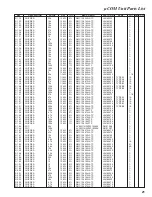
Страница 29: ...92 1 C 336 CHIP CAP 0 001uF 50V B GRM188B11H102KA01D K22174821 1 C 337 CHIP CAP 0 001uF 50V B GRM188B11H102KA01D K22174821 1 C 338 CHIP CAP 0 001uF 50V B GRM188B11H102KA01D K22174821 1 C 339 CHIP CAP...

Страница 30: ...CAP 0 001uF 50V B GRM188B11H102KA01D K22174821 1 C 408 CHIP CAP 0 001uF 50V B GRM188B11H102KA01D K22174821 1 C 409 AL ELECTRO CAP EMV 250ADA4R7MB55G S8101397 1 C 410 CHIP CAP 100pF 50V CH GRM1882C1H10...

Страница 31: ...1 C 483 CHIP CAP 0 01uF 50V B GRM188B11H103KA01D K22174823 1 C 484 CHIP CAP 0 01uF 50V B GRM188B11H103JA01D K22174824 TYPE B3 19 C 485 CHIP CAP 0 001uF 50V B GRM188B11H102KA01D K22174821 1 C 486 CHIP...

Страница 32: ...188B11H103KA01D K22174823 50 C 563 CHIP CAP 10pF 50V CH GRM1882C1H100JA01D K22174211 51 C 564 CERAMIC CAP 0 001uF 50V B UP050B102K A B K28179001 70 D 301 SURGE ABSORBER P6KE18A Q9000630 1 D 302 DIODE...

Страница 33: ...7uH LK1608 4R7K T L1690688 1 L 342 INDUCTOR MLF1608DR22KT S8101412 1 L 343 M RFC 0 0056uH LL1608 FSL5N6S L1690858 TYPE B1 19 L 343 M RFC 0 0056uH LL1608 FSL5N6S L1690858 TYPE B2 19 Q 301 TRANSISTOR 2S...

Страница 34: ...5 RMC1 16 471JATP J24185471 1 R 335 CHIP RES 5 6k 1 16W 5 RMC1 16 562JATP J24185562 1 R 336 CHIP RES 220 1 16W 5 RMC1 16 221JATP J24185221 1 R 337 CHIP RES 4 7k 1 16W 5 RMC1 16 472JATP J24185472 1 R 3...

Страница 35: ...47k 1 16W 5 RMC1 16 473JATP J24185473 1 R 406 CHIP RES 2 7k 1 16W 5 RMC1 16 272JATP J24185272 1 R 407 CHIP RES 220k 1 16W 5 RMC1 16 224JATP J24185224 1 R 408 CHIP RES 470k 1 16W 5 RMC1 16 474JATP J24...

Страница 36: ...IP RES 22k 1 16W 5 RMC1 16 223JATP J24185223 37 R 476 CHIP RES 10k 1 16W 5 RMC1 16 103JATP J24185103 1 R 477 CHIP RES 10k 1 16W 5 RMC1 16 103JATP J24185103 1 R 479 CHIP RES 4 7k 1 16W 5 RMC1 16 472JAT...

Страница 37: ...M 1 16W 5 RMC1 16 225JATP J24185225 1 R 518 THERMISTOR TBPS1R473J475H5Q S8101388 1 R 519 CHIP RES 0 1 16W 5 RMC1 16 000JATP J24185000 1 R 520 CHIP RES 560k 1 10W 5 RMC1 10T 564J J24205564 1 R 521 CHIP...

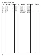
Страница 38: ...38 REF DESCRIPTION VALUE V W TOL MFR S DESIG VXSTD P N VERS LOT SIDE LAY ADR Note...

Страница 39: ...13...

Страница 40: ...14 Copyright 2007 VERTEX STANDARD CO LTD All rights reserved No portion of this manual may be reproduced without the permission of VERTEX STANDARD CO LTD Printed in Japan...

Отзывы: