


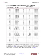


ZC706 Evaluation Board User Guide
15
UG954 (v1.5) September 10, 2015
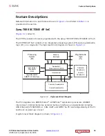
Feature Descriptions
For additional information on Zynq-7000 SoC devices, see
Zynq-7000 All Programmable
SoC Overview (
)
and
Zynq-7000 All Programmable SoC Technical Reference Manual
(
).
Device Configuration
the Zynq-7000 XC7Z045 AP SoC uses a multi-stage boot process that supports both a
non-secure and a secure boot. The PS is the master of the boot and configuration process.
For a secure boot, the PL must be powered on to enable the use of the security block
located within the PL, which provides 256-bit AES and SHA decryption/authentication.
The ZC706 evaluation board supports these configuration options:
• PS Configuration: Quad-SPI flash memory
• PS Configuration: Processor System Boot from SD Card (J30)
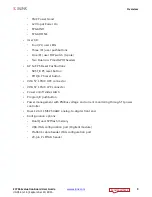
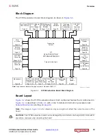
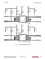
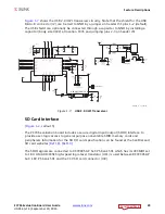
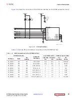
X-Ref Target - Figure 1-4
Figure 1-4:
Zynq-7000 Block Diagram
2x USB
2x GigE
2x SD
Zynq-7000 AP SoC
I/O
Peripherals
IRQ
IRQ
EMIO
SelectIO
Resources
DMA 8
Channel
CoreSight
Components
Programmable Logic
DAP
DevC
SWDT
DMA
Sync
Notes:
1) Arrow direction shows control (master to slave)
2) Data flows in both directions:
AXI 32-Bit/64-Bit
,
AXI 64-Bit
,
AXI 32-Bit,
AHB 32-Bit,
APB 32-Bit
, Custom
ACP
256K
SRAM
Application Processor Unit
TTC
System-
Level
Control
Regs
GigE
CAN
SD
SDIO
UART
GPIO
UART
CAN
I2C
SRAM/
NOR
ONFI 1.0
NAND
Processing System
Memory
Interfaces
Q-SPI
CTRL
USB
GigE
I2C
USB
SD
SDIO
SPI
SPI
Programmable Logic to
Memory Interconnect
MMU
FPU and NEON Engine
Snoop Controller, AWDT, Timer
GIC
32 KB
I-Cache
ARM Cortex-A9
CPU
ARM Cortex-A9
CPU
MMU
FPU and NEON Engine
Config
AES/
SHA
XADC
12-Bit ADC
Memory
Interfaces
512 KB L2 Cache & Controller
OCM
Interconnect
DDR2/3,
LPDDR2
Controller
UG954_c1_04_100112
32 KB
D-Cache
32 KB
I-Cache
32 KB
D-Cache
MIO
Clock
Generation
Reset
Central
Interconnect
General-Purpose
Ports
High-Performance Ports


