background image

36

www.xilinx.com

VC707 Evaluation Board

UG885 (v1.2) February 1, 2013

Chapter 1:

VC707 Evaluation Board Features

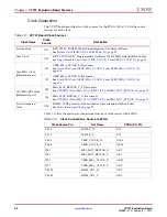
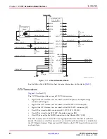
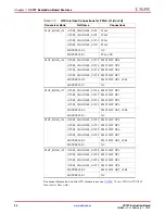
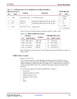
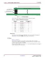
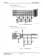
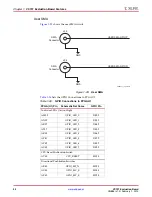
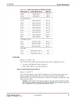
Table 1-15

 lists the SFP+ module RX and TX connections to the FPGA.

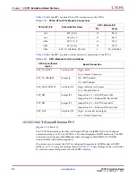
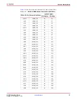
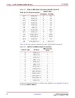
Table 1-16

 lists the SFP+ module control and status connections to the FPGA.

10/100/1000 Tri-Speed Ethernet PHY

[

Figure 1-2

, callout 

15

]

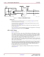
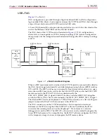
The VC707 board utilizes the Marvell Alaska PHY device (88E1111) U50 for Ethernet 
communications at 10, 100, or 1000 Mb/s. The board supports SGMII mode only. The PHY 
connection to a user-provided Ethernet cable is through a Halo HFJ11-1G01E RJ-45 
connector (P4) with built-in magnetics.

On power-up, or on reset, the PHY is configured to operate in SGMII mode with PHY 
address 

0b00111

 using the settings shown in 

Table 1-17

. These settings can be overwritten 

by software commands passed over the MDIO interface.

Table 1-15:

FPGA U1 to SFP+ Module Connections

FPGA (U1) Pin

Schematic Net Name

SFP+ Module (P3)

Pin

Name

AL5

SFP_RX_N

12

RD_N

AL6

SFP_RX_P

13

RD_P

AM4

SFP_TX_P

18

TD_P

AM3

SFP_TX_N

19

TD_N

AP33

SFP_TX_DISABLE_TRANS

3

TX_DISABLE

Table 1-16:

SFP+ Module Control and Status

SFP Control/Status

Signal

Board Connection

SFP_TX_FAULT

Test Point J22

High = Fault

Low = Normal Operation

SFP_TX_DISABLE

Jumper J6

Off = SFP Disabled

On = SFP Enabled

SFP_MOD_DETECT

Test Point J21

High = Module Not Present

Low = Module Present

SFP_RS0

Jumper J38

Jumper Pins 1-2 = Full RX Bandwidth

Jumper Pins 2-3 = Reduced RX Bandwidth

SFP_RS1

Jumper J39

Jumper Pins 1-2 = Full TX Bandwidth

Jumper Pins 2-3 = Reduced TX Bandwidth

SFP_LOS

Test Point J20

High = Loss of Receiver Signal

Low = Normal Operation

Содержание VC707

Страница 1: ...VC707 Evaluation Board for the Virtex 7 FPGA User Guide UG885 v1 2 February 1 2013...

Страница 2: ...ther countries PCI PCI Express PCIe and PCI X are trademarks of PCI SIG HDMI HDMI logo and High Definition Multimedia Interface are trademarks of HDMI Licensing LLC All other trademarks are the proper...

Страница 3: ...ector 35 10 100 1000 Tri Speed Ethernet PHY 36 SGMII GTX Transceiver Clock Generation 37 USB to UART Bridge 38 HDMI Video Output 39 LCD Character Display 16 x 2 43 I2C Bus 44 Status LEDs 46 User I O 4...

Страница 4: ...ications Dimensions 95 Environmental 95 Temperature 95 Humidity 95 Operating Voltage 95 Appendix F Additional Resources Xilinx Resources 97 Solution Centers 97 Further Resources 97 References 98 Appen...

Страница 5: ...07 Board Features for a complete list of features The details for each feature are described in Feature Descriptions page 7 Additional Information See Appendix F Additional Resources for references to...

Страница 6: ...or FMC2 HPC connector SFP connector I2C programmable jitter attenuating precision clock multiplier Status LEDs Ethernet status Power good FPGA INIT FPGA DONE User I O User LEDs eight GPIO User pushbut...

Страница 7: ...umbered feature that is referenced in Figure 1 2 is described in the sections that follow Note The image in Figure 1 2 is for reference only and might not reflect the current revision of the board X R...

Страница 8: ...fan XC7VX485T 2FFG1761C 2 J1 DDR3 SODIMM memory 1 GB Micron MT8JTF12864HZ 1G6G1 21 3 U3 BPI parallel NOR flash memory 1 Gb Micron Numonyx PC28F00AG18FE 35 4 U8 J2 USB ULPI transceiver USB mini B conn...

Страница 9: ...7 AD ADV7511KSTZ P 43 42 19 J23 LCD character display and connector 2 x 7 0 1 inch male header 39 20 U52 I2C Bus Switch back side of board TI PCA9548ARGER 41 21 DS11 DS13 Ethernet status LEDs EPHY sta...

Страница 10: ...Sixteen I O banks are available on the VC707 board bank 31 is not used The voltages applied to the FPGA I O banks used by the VC707 board are listed in Table 1 3 X Ref Target Figure 1 3 Figure 1 3 SW1...

Страница 11: ...ace banks 37 and 39 Any interface connected to these banks that requires a reference voltage must use this FPGA voltage reference The connections between the DDR3 memory and the FPGA are listed in Tab...

Страница 12: ...DQ0 N13 DDR3_D1 7 DQ1 L14 DDR3_D2 15 DQ2 M14 DDR3_D3 17 DQ3 M12 DDR3_D4 4 DQ4 N15 DDR3_D5 6 DQ5 M11 DDR3_D6 16 DQ6 L12 DDR3_D7 18 DQ7 K14 DDR3_D8 21 DQ8 K13 DDR3_D9 23 DQ9 H13 DDR3_D10 33 DQ10 J13 DD...

Страница 13: ...DDR3_D34 141 DQ34 B26 DDR3_D35 143 DQ35 A22 DDR3_D36 130 DQ36 B22 DDR3_D37 132 DQ37 A25 DDR3_D38 140 DQ38 C24 DDR3_D39 142 DQ39 E24 DDR3_D40 147 DQ40 D23 DDR3_D41 149 DQ41 D26 DDR3_D42 157 DQ42 C25 D...

Страница 14: ...DM2 A14 DDR3_DM3 63 DM3 C23 DDR3_DM4 136 DM4 D25 DDR3_DM5 153 DM5 C31 DDR3_DM6 170 DM6 F31 DDR3_DM7 187 DM7 M16 DDR3_DQS0_N 10 DQS0_N N16 DDR3_DQS0_P 12 DQS0_P J12 DDR3_DQS1_N 27 DQS1_N K12 DDR3_DQS1_...

Страница 15: ...y voltage 1 8V Datapath width 16 bits 26 address lines and 7 control signals Data rate Up to 40 MHz The Linear BPI Flash memory can synchronously configure the FPGA in Master BPI mode at the 40 MHz da...

Страница 16: ...n the flash memory 1 of the 4 bitstreams can be selected to configure the FPGA by appropriately setting the DIP switch SW11 The connections between the BPI Flash memory and the FPGA are listed in Tabl...

Страница 17: ...y on the VC707 board For more details see the Numonyx PC28F00AG18FE data sheet Ref 1 AW41 FLASH_A25 B8 A26 NA NC H1 A27 AM36 FLASH_D0 F2 DQ0 AN36 FLASH_D1 E2 DQ1 AJ36 FLASH_D2 G3 DQ2 AJ37 FLASH_D3 E4...

Страница 18: ...8 x 10 mm U3 FLASH_A0 A1 FLASH_A1 A2 FLASH_A2 A3 FLASH_A3 A4 FLASH_A4 A5 FLASH_A5 A6 FLASH_A6 A7 FLASH_A7 A8 FLASH_A8 A9 FLASH_A9 A10 FLASH_A10 A11 FLASH_A11 A12 FLASH_A12 A13 FLASH_A13 A14 FLASH_A14...

Страница 19: ...s the shield for the USB mini B connector J2 can be tied to GND by a jumper on header J44 pins 1 2 default The USB shield can optionally be connected through a capacitor to GND by installing a tantalu...

Страница 20: ...C REFSEL1 DATA6 DATA5 DATA4 DATA3 19 18 23 21 24 20 VDD33_P VBAT RBIAS ID DP DM 14 15 SPK_L REFSEL2 33 CTR_GND USB_SMSC_NXT USB_SMSC_DATA0 USB_SMSC_DATA1 USB_SMSC_DATA2 USB_SMSC_DATA3 USB_SMSC_DATA4 U...

Страница 21: ..._P NC 12 GNDTAB3 GNDTAB4 IOGND1 IOGND2 15 16 17 18 13 14 51 1K 1 Six Places VCC3V3 R318 R319 R316 R317 R314 R315 2 VCC1V8 C51 0 1 F 25V X5R GND GND VCC3V3 C50 0 1 F 25V X5R GND SDIO_DAT2_LS SDIO_DAT1_...

Страница 22: ...en an FMC mezzanine card is attached Switch U27 adds an attached FMC1 HPC mezzanine card to the FPGAs JTAG chain as determined by the FMC_HPC_PRSNT_M2C_B signal Switch U28 adds an attached FMC2 HPC da...

Страница 23: ...FMC1_HPC_TCK_BUF FPGA_TDI_BUF FMC2_PRSNT_M2C_B_LS FMC1_PRSNT_M2C_B_LS FMC1 HPC Connector TDI TDO J35 TMS TCK PRSNT_L VCC3V3 FMC2 HPC Connector TDI TDO J37 TMS TCK PRSNT_L Virtex 7 FPGA TDI TDO U1 TMS...

Страница 24: ...ntial pair J31 USER_SMA_CLOCK_P Net name See User SMA Clock USER_SMA_CLOCK_P and USER_SMA_CLOCK_N page 26 J32 USER_SMA_CLOCK_N Net name See User SMA Clock USER_SMA_CLOCK_P and USER_SMA_CLOCK_N page 26...

Страница 25: ...d has a programmable low jitter 3 3V differential oscillator U34 connected to the FPGA MRCC inputs of bank 14 This USER_CLOCK_P and USER_CLOCK_N clock signal pair are connected to FPGA U1 pins AK34 an...

Страница 26: ...k signal names are USER_SMA_CLOCK_P and USER_SMA_CLOCK_N which are connected to FPGA U1 pins AJ32 and AK32 respectively The user provided 1 8 V differential clock circuit is shown in Figure 1 11 X Ref...

Страница 27: ...ement a clock recovery circuit and then output this clock to a differential I O pair on I O bank 13 REC_CLOCK_C_P FPGA U1 pin AW32 and REC_CLOCK_C_N FPGA U1 pin AW33 for jitter attenuation The jitter...

Страница 28: ...lock for a Quad can be sourced from the Quad above or Quad below the GTX Quad of interest There are four GTX Quads on the VC707 board with connectivity as shown here X Ref Target Figure 1 13 Figure 1...

Страница 29: ...DP4 DP7 Quad 117 MGTREFCLK0 FMC2 HPC GBTCLK0 Contains 4 GTX transceivers for FMC2 HPC DP0 DP3 Quad 118 MGTREFCLK0 FMC1 HPC GBTCLK1 Contains 4 GTX transceivers for FMC1 HPC DP4 DP7 Quad 119 MGTREFCLK0...

Страница 30: ...P7 MGTREFCLK0 FMC2 HPC GBT_CLK1 MGTREFCLK1 NC MGT_BANK_117 GTXE2_CHANNEL_X1Y16 FMC2 HPC DP0 GTXE2_CHANNEL_X1Y17 FMC2 HPC DP1 GTXE2_CHANNEL_X1Y18 FMC2 HPC DP2 GTXE2_CHANNEL_X1Y19 FMC2 HPC DP3 MGTREFCLK...

Страница 31: ...1 and 2 jumpered Table 1 12 lists the PCIe edge connector connections at P1 X Ref Target Figure 1 14 Figure 1 14 PCI Express Clock X Ref Target Figure 1 15 Figure 1 15 PCI Express Lane Size Select Ju...

Страница 32: ...t pair GTXE2_CHANNEL_X0Y17 PCIE_TX2_N AC1 A26 PERn2 Integrated Endpoint block transmit pair GTXE2_CHANNEL_X0Y17 PCIE_TX3_P AE2 A29 PERp3 Integrated Endpoint block transmit pair GTXE2_CHANNEL_X0Y16 PCI...

Страница 33: ...AA6 PCIE_RX1_P B19 PETp1 GTXE2_CHANNEL_X0Y18 MGTXRXN2_115_AA5 AA5 PCIE_RX1_N B20 PETn1 GTXE2_CHANNEL_X0Y18 MGTXTXP3_115_W2 W2 PCIE_TX0_P A16 PERp0 GTXE2_CHANNEL_X0Y19 MGTXTXN3_115_W1 W1 PCIE_TX0_N A1...

Страница 34: ...XN2_114_AH3 AH3 PCIE_TX5_N A40 PERn5 GTXE2_CHANNEL_X0Y14 MGTXRXP2_114_AE6 AE6 PCIE_RX5_P B37 PETp5 GTXE2_CHANNEL_X0Y14 MGTXRXN2_114_AE5 AE5 PCIE_RX5_N B38 PETn5 GTXE2_CHANNEL_X0Y14 MGTXTXP3_114_AG2 AG...

Страница 35: ...X SFP Enable 1 2 FULL BW TX SFP_RS1 SFP_VCCT 32 21 22 23 24 25 26 27 28 29 30 19 18 16 15 13 12 8 20 17 14 10 11 1 7 9 6 5 4 3 2 31 P3 SFP Module Connector 74441 0010 SFP_LOS SFP_TX_FAULT SFP_IIC_SDA...

Страница 36: ...0111 using the settings shown in Table 1 17 These settings can be overwritten by software commands passed over the MDIO interface Table 1 15 FPGA U1 to SFP Module Connections FPGA U1 Pin Schematic Net...

Страница 37: ...the Ethernet SGMII clock source Table 1 17 Board Connections for PHY Configuration Pins Pin Connection on Board Bit 2 Definition and Value Bit 1 Definition and Value Bit 0 Definition and Value CFG0 VC...

Страница 38: ...ble is plugged into the USB port on the VC707 board Xilinx UART IP is expected to be implemented in the FPGA fabric The FPGA supports the USB to UART bridge using four signal pins Transmit TX Receive...

Страница 39: ...put data mapping The VC707 board supports the following HDMI device interfaces 36 data lines Independent VSYNC HSYNC Single ended input CLK Interrupt Out Pin to FPGA I2C SPDIF Table 1 19 USB Connector...

Страница 40: ...9 19 1 30 U48 ADV7511 HDMI_D10 VADJ HDMI_HEAC_C_N HDMI_AVDD HDMI_PLVDD HDMI_PLVDD 2 1 X5R 25V 0 1UF C78 HDMI_CLK HDMI_HSYNC HDMI_VSYNC HDMI_INT 1 1 1 10W 2 43K R105 R106 2 43K 1 10W 1 IIC_SCL_HDMI 1 2...

Страница 41: ...DMI_D4 92 D4 AL21 HDMI_D5 91 D5 AK22 HDMI_D6 90 D6 AJ22 HDMI_D7 89 D7 AL20 HDMI_D8 88 D8 AK20 HDMI_D9 87 D9 AK23 HDMI_D10 86 D10 AJ23 HDMI_D11 85 D11 AN21 HDMI_D12 84 D12 AP22 HDMI_D13 83 D13 AP23 HDM...

Страница 42: ...57 D35 AP21 HDMI_DE 97 DE AR23 HDMI_SPDIF 10 SPDIF AU23 HDMI_CLK 79 CLK AT22 HDMI_VSYNC 2 VSYNC AU22 HDMI_HSYNC 98 HSYNC AM24 HDMI_INT 45 INT AR22 HDMI_SPDIF_OUT 46 SPDIF_OUT Table 1 22 ADV7511 to HDM...

Страница 43: ...header shown in Figure 1 21 When the LCD is not installed the J31 header pins listed in Table 1 23 are available for use as GPIO X Ref Target Figure 1 19 Figure 1 19 LCD Display UG885_c1_19_020612 LCD...

Страница 44: ...L which is routed through a 1 to 8 channel I2C bus switch U52 The bus switch can operate at speeds up to 400 kHz The bus switch I2C address is 0x74 0b01110100 and must be addressed and configured to s...

Страница 45: ...ology Table 1 24 I2C Bus Addresses I2C Bus I2C Switch Position I2C Address PCA9548 NA 0b1110100 USER_CLK_SDL SCL 0 0b1110000 FMC1_HPC_IIC_SDA SCL 1 0bXXXXX00 FMC2_HPC_IIC_SDA SCL 2 0bXXXXX00 EEPROM_II...

Страница 46: ...D character display callout 19 If the display is unmounted connector J23 pins are available as 7 independent GPIOs The LCD connector J23 details are shown in the LCD Character Display 16 x 2 section T...

Страница 47: ...it X Ref Target Figure 1 23 Figure 1 23 User LEDs UG855_c1_23_020612 R147 49 9 1 DS2 R148 49 9 1 DS3 R149 49 9 1 DS4 R150 49 9 1 DS5 R151 49 9 1 DS6 R152 49 9 1 DS7 R153 49 9 1 DS8 R154 49 9 1 GND DS9...

Страница 48: ...er pushbutton switch circuits X Ref Target Figure 1 25 Figure 1 25 User Pushbuttons VCC1V8 GPIO SW N R36 4 7k 0 1 W 5 GND 4 3 2 1 SW3 VCC1V8 GPIO SW W R40 4 7k 0 1 W 5 GND 4 3 2 1 SW7 VADJ GPIO SW C R...

Страница 49: ...PIO_DIP_SW5 GPIO_DIP_SW6 GPIO_DIP_SW7 R46 4 7k 0 1 W 5 R47 4 7k 0 1 W 5 R48 4 7k 0 1 W 5 R49 4 7k 0 1 W 5 12 11 10 9 1 2 3 4 GND 5 6 7 8 GPIO_DIP_SW0 GPIO_DIP_SW1 GPIO_DIP_SW2 GPIO_DIP_SW3 R53 4 7k 0...

Страница 50: ...A U1 FPGA U1 Pin Schematic Net Name GPIO Pin Indicator LEDs Active High AM39 GPIO_LED_0 DS2 2 AN39 GPIO_LED_1 DS3 2 AR37 GPIO_LED_2 DS4 2 AT37 GPIO_LED_3 DS5 2 AR35 GPIO_LED_4 DS6 2 AP41 GPIO_LED_5 DS...

Страница 51: ...ls on the onboard power system Caution Do NOT plug a PC ATX power supply 6 pin connector into J18 on the VC707 board The ATX 6 pin connector has a different pinout than J18 Connecting an ATX 6 pin con...

Страница 52: ...rcegate Technologies part number AZCBL WH 1109 RA4 Figure 1 30 shows the power connector J18 power switch SW12 and indicator LED DS16 X Ref Target Figure 1 29 Figure 1 29 ATX Power Supply Adapter Cabl...

Страница 53: ...Upper Linear Flash Address Switch SW11 Figure 1 2 callout 29 FPGA Configuration Mode DIP switch SW11 positions 3 4 and 5 control which configuration mode is used at power up or when the PROG pushbutt...

Страница 54: ...lly populated with all 400 pins present The LPC version is partially populated with 160 pins The 10 x 40 rows of an FMC HPC connector provides pins for up to 160 single ended or 80 differential user d...

Страница 55: ...version is partially populated with 160 pins The 10 x 40 rows of an FMC HPC connector provides pins for up to 160 single ended or 80 differential user defined signals 10 GTX transceivers 2 GTX clocks...

Страница 56: ..._M2C_P C6 B1 NC A3 FMC1_HPC_DP1_M2C_N C5 B4 NC A6 FMC1_HPC_DP2_M2C_P B8 B5 NC A7 FMC1_HPC_DP2_M2C_N B7 B8 NC A10 FMC1_HPC_DP3_M2C_P A6 B9 NC A11 FMC1_HPC_DP3_M2C_N A5 B12 FMC1_HPC_DP7_M2C_P E6 A14 FMC...

Страница 57: ...C19 FMC1_HPC_LA14_N N40 D17 FMC1_HPC_LA13_P H39 C22 FMC1_HPC_LA18_CC_P M32 D18 FMC1_HPC_LA13_N G39 C23 FMC1_HPC_LA18_CC_N L32 D20 FMC1_HPC_LA17_CC_P L31 C26 FMC1_HPC_LA27_P J31 D21 FMC1_HPC_LA17_CC_N...

Страница 58: ..._HA15_N C34 E19 FMC1_HPC_HA20_N A34 F19 FMC1_HPC_HA19_P B32 E21 FMC1_HPC_HB03_P G28 F20 FMC1_HPC_HA19_N B33 E22 FMC1_HPC_HB03_N G29 F22 FMC1_HPC_HB02_P K28 E24 FMC1_HPC_HB05_P K27 F23 FMC1_HPC_HB02_N...

Страница 59: ..._LA16_N K38 H17 FMC1_HPC_LA11_N F41 G21 FMC1_HPC_LA20_P Y29 H19 FMC1_HPC_LA15_P M36 G22 FMC1_HPC_LA20_N Y30 H20 FMC1_HPC_LA15_N L37 G24 FMC1_HPC_LA22_P R28 H22 FMC1_HPC_LA19_P W30 G25 FMC1_HPC_LA22_N...

Страница 60: ...MC1_HPC_HA14_N E38 K16 FMC1_HPC_HA17_CC_P C35 J18 FMC1_HPC_HA18_P F39 K17 FMC1_HPC_HA17_CC_N C36 J19 FMC1_HPC_HA18_N E39 K19 FMC1_HPC_HA21_P D37 J21 FMC1_HPC_HA22_P F36 K20 FMC1_HPC_HA21_N D38 J22 FMC...

Страница 61: ..._DP1_C2M_N M3 B24 NC A26 FMC2_HPC_DP2_C2M_P L2 B25 NC A27 FMC2_HPC_DP2_C2M_N L1 B28 NC A30 FMC2_HPC_DP3_C2M_P K4 B29 NC A31 FMC2_HPC_DP3_C2M_N K3 B32 FMC2_HPC_DP7_C2M_P R6 A34 FMC2_HPC_DP4_C2M_P U2 B3...

Страница 62: ...D33 F4 FMC2_HPC_HA00_CC_P AB33 E6 FMC2_HPC_HA05_P Y32 F5 FMC2_HPC_HA00_CC_N AC33 E7 FMC2_HPC_HA05_N Y33 F7 FMC2_HPC_HA04_P AB29 E9 FMC2_HPC_HA09_P AE29 F8 FMC2_HPC_HA04_N AC29 E10 FMC2_HPC_HA09_N AE30...

Страница 63: ...10 FMC2_HPC_LA03_N AK42 H8 FMC2_HPC_LA02_N AL39 G12 FMC2_HPC_LA08_P AD42 H10 FMC2_HPC_LA04_P AL41 G13 FMC2_HPC_LA08_N AE42 H11 FMC2_HPC_LA04_N AL42 G15 FMC2_HPC_LA12_P Y39 H13 FMC2_HPC_LA07_P AC40 G16...

Страница 64: ..._CC_N AD35 J19 FMC2_HPC_HA18_N AB37 K19 FMC2_HPC_HA21_P AA34 J21 FMC2_HPC_HA22_P Y35 K20 FMC2_HPC_HA21_N AA35 J22 FMC2_HPC_HA22_N AA36 K22 FMC2_HPC_HA23_P Y37 J24 FMC2_HPC_HB01_P AM16 K23 FMC2_HPC_HA2...

Страница 65: ...VCC12_P Power Plane From SW12 MGTAVCC VCCINT VCCAUX_IO VCCBRAM MGTVCCAUX Power Controller 2 Aux PMBus Address 53 Switching Regulator 1 5V at 10A U21 Switching Regulator 2 5V at 10A Switching Regulato...

Страница 66: ...voltage controller and regulators UCD9248PFC 2 U43 PMBus Controller Addr 53 50 PTD08D210W VOUT A U21 Adjustable switching regulator dual 10A 0 6Vto 3 6V VCC2V5_FPGA 2 50V 51 PTD08D210W VOUT B Adjusta...

Страница 67: ...at J51 after a VC707 board powers up in this mode turns on the FMC_VADJ rail Documentation describing PMBUS programming for the UCD9248 digital power controller is available at the Texas Instruments w...

Страница 68: ...5 5 1 2 07 10 41 90 3 Rail 3 VCC3V3 3 3 2 97 2 805 0 5 4 1 3 795 10 41 90 4 Rail 4 VADJ 1 8 1 62 1 53 0 5 3 1 2 07 10 41 90 Notes 1 The values defined in these columns are the voltage current and temp...

Страница 69: ...the VC707 board are operating at moderate to high current levels due to a customer design the modules can generate substantial heat which can cause them to shut down without warning The power module s...

Страница 70: ...uxiliary analog input channels Simultaneous sampling of Channel 0 and Channel 8 is supported A user provided analog signal multiplexer card can be used to sample additional external analog inputs usin...

Страница 71: ..._GPIO_0 XADC_GPIO_2 XADC_GPIO_1 XADC_GPIO_3 J19 1 3 5 7 9 11 13 15 17 19 2 4 6 8 10 12 14 16 18 20 GND XADC_AGND XADC_AGND XADC_VCC5V0 VADJ Table 1 33 XADC Header J19 Pinout Net Name J19 Pin Number De...

Страница 72: ...ation speed an external 80 MHz oscillator is wired to the EMCCLK pin of the FPGA This allows users to create bitstreams that configure the FPGA over the 16 bit datapath from the Linear BPI Flash memor...

Страница 73: ...18FE 1Gb Flash Memory TCK TMS TDI TDO Bank 0 VCCO 1 8V CCLK INIT_B VBATT M 2 0 DONE PROG_B U1 FPGA SW9 Bank 15 VCCO 1 8V Bank 14 VCCO 1 8V FWE_B FOE_B ADV_B RS1 RS0 A 26 25 A 23 16 A 15 00 D 15 00 FCS...

Страница 74: ...74 www xilinx com VC707 Evaluation Board UG885 v1 2 February 1 2013 Chapter 1 VC707 Evaluation Board Features...

Страница 75: ...are shown in Figure A 1 and details are listed in Table A 1 X Ref Target Figure A 1 Figure A 1 SW2 Default Settings Table A 1 SW2 Default Switch Settings Position Function Default 1 GPIO_DIP_SW0 Off...

Страница 76: ...Default Switch Settings Position Function Default 1 FLASH_A25 A25 Off 2 FLASH_A24 A24 Off 3 FPGA_M2 M0 Off 4 FPGA_M1 M1 On 5 FPGA_M0 M3 Off UG885_aB_02_020612 1 OFF Position 0 ON Position 1 2 3 4 5 A2...

Страница 77: ...D jumper None J45 USB SMBC U8 VBUS 1 2 J49 PCIe Bus Width Select Header 1 2 J50 TI Controller U64 Addr 54 Reset jumper None J51 FMC_VADJ_ON_B jumper 1 2 J52 FPGA U1 INIT_B to PROG_B jumper None J53 XA...

Страница 78: ...78 www xilinx com VC707 Evaluation Board UG885 v1 2 February 1 2013 Appendix A Default Switch and Jumper Settings...

Страница 79: ...M_P DP2_C2M_N GND GND DP3_C2M_P DP3_C2M_N GND GND DP4_C2M_P DP4_C2M_N GND GND DP5_C2M_P DP5_C2M_N GND RES1 GND GND DP9_M2C_P DP9_M2C_N GND GND DP8_M2C_P DP8_M2C_N GND GND DP7_M2C_P DP7_M2C_N GND GND D...

Страница 80: ...M_P DP2_C2M_N GND GND DP3_C2M_P DP3_C2M_N GND GND DP4_C2M_P DP4_C2M_N GND GND DP5_C2M_P DP5_C2M_N GND RES1 GND GND DP9_M2C_P DP9_M2C_N GND GND DP8_M2C_P DP8_M2C_N GND GND DP7_M2C_P DP7_M2C_N GND GND D...

Страница 81: ...CCO VCC1V8_FPGA IO_L5P_T0_13 NET USB_SMSC_DIR LOC BB33 IOSTANDARD LVCMOS18 Bank 13 VCCO VCC1V8_FPGA IO_L5N_T0_13 NET USB_SMSC_DATA7 LOC AW35 IOSTANDARD LVCMOS18 Bank 13 VCCO VCC1V8_FPGA IO_L6P_T0_13 N...

Страница 82: ...1V8_FPGA IO_L12P_T1_MRCC_14 NET USER_CLOCK_N LOC AL34 IOSTANDARD LVDS Bank 14 VCCO VCC1V8_FPGA IO_L12N_T1_MRCC_14 NET USER_SMA_CLOCK_P LOC AJ32 IOSTANDARD LVCMOS18 Bank 14 VCCO VCC1V8_FPGA IO_L13P_T2_...

Страница 83: ...T FMC2_HPC_HA15_N LOC AF37 IOSTANDARD LVCMOS18 Bank 16 VCCO VADJ_FPGA IO_L2N_T0_16 NET FMC2_HPC_HA12_P LOC AF34 IOSTANDARD LVCMOS18 Bank 16 VCCO VADJ_FPGA IO_L3P_T0_DQS_16 NET FMC2_HPC_HA12_N LOC AG34...

Страница 84: ...DJ_FPGA IO_L17N_T2_17 NET FMC2_HPC_LA09_P LOC AJ38 IOSTANDARD LVCMOS18 Bank 17 VCCO VADJ_FPGA IO_L18P_T2_17 NET FMC2_HPC_LA09_N LOC AK38 IOSTANDARD LVCMOS18 Bank 17 VCCO VADJ_FPGA IO_L18N_T2_17 NET 5N...

Страница 85: ...G41 IOSTANDARD LVCMOS18 Bank 19 VCCO VADJ_FPGA IO_L9P_T1_DQS_19 NET FMC1_HPC_LA07_N LOC G42 IOSTANDARD LVCMOS18 Bank 19 VCCO VADJ_FPGA IO_L9N_T1_DQS_19 NET FMC1_HPC_LA11_P LOC F40 IOSTANDARD LVCMOS18...

Страница 86: ...LVCMOS18 Bank 33 VCCO VCC1V8_FPGA IO_L23N_T3_33 NET XADC_GPIO_2 LOC BB24 IOSTANDARD LVCMOS18 Bank 33 VCCO VCC1V8_FPGA IO_L24P_T3_33 NET XADC_GPIO_3 LOC BB23 IOSTANDARD LVCMOS18 Bank 33 VCCO VCC1V8_FPG...

Страница 87: ...O VADJ_FPGA IO_L14P_T2_SRCC_35 NET FMC1_HPC_HA21_N LOC D38 IOSTANDARD LVCMOS18 Bank 35 VCCO VADJ_FPGA IO_L14N_T2_SRCC_35 NET FMC1_HPC_HA05_P LOC G32 IOSTANDARD LVCMOS18 Bank 35 VCCO VADJ_FPGA IO_L15P_...

Страница 88: ...V5_FPGA IO_L3N_T0_DQS_37 NET DDR3_DM4 LOC C23 IOSTANDARD SSTL15 Bank 37 VCCO VCC1V5_FPGA IO_L4P_T0_37 NET DDR3_D33 LOC B23 IOSTANDARD SSTL15 Bank 37 VCCO VCC1V5_FPGA IO_L4N_T0_37 NET DDR3_D35 LOC B26...

Страница 89: ...RD SSTL15 Bank 38 VCCO VCC1V5_FPGA IO_L20P_T3_38 NET 10N484 LOC L17 IOSTANDARD SSTL15 Bank 38 VCCO VCC1V5_FPGA IO_L20N_T3_38 NET 10N485 LOC N19 IOSTANDARD SSTL15 Bank 38 VCCO VCC1V5_FPGA IO_L21P_T3_DQ...

Страница 90: ...111 MGTREFCLK1P_111 NET 12N123 LOC BA2 Bank 111 MGTXTXP1_111 NET GND LOC BA6 Bank 111 MGTXRXP1_111 NET 12N122 LOC BA1 Bank 111 MGTXTXN1_111 NET GND LOC BA5 Bank 111 MGTXRXN1_111 NET 12N125 LOC BB4 Ban...

Страница 91: ..._DP7_M2C_P LOC R6 Bank 116 MGTXRXP3_116 NET FMC2_HPC_DP7_C2M_N LOC P3 Bank 116 MGTXTXN3_116 NET FMC2_HPC_DP7_M2C_N LOC R5 Bank 116 MGTXRXN3_116 NET FMC2_HPC_DP6_C2M_P LOC R2 Bank 116 MGTXTXP2_116 NET...

Страница 92: ...MGTXRXP0_118 NET FMC1_HPC_DP4_C2M_N LOC J1 Bank 118 MGTXTXN0_118 NET FMC1_HPC_DP4_M2C_N LOC H7 Bank 118 MGTXRXN0_118 NET FMC1_HPC_DP3_C2M_P LOC B4 Bank 119 MGTXTXP3_119 NET FMC1_HPC_DP3_M2C_P LOC A6 B...

Страница 93: ...n the PC chassis following the instructions provided with the PC 4 Select a vacant PCIe expansion slot and remove the expansion cover at the back of the chassis by removing the screws on the top and b...

Страница 94: ...94 www xilinx com VC707 Evaluation Board UG885 v1 2 February 1 2013 Appendix D Board Setup...

Страница 95: ...cations Dimensions Height 5 5 inch 14 0 cm Length 10 5 inch 26 7 cm Note The VC707 board height exceeds the standard 4 376 inch 11 15 cm height of a PCI Express card Environmental Temperature Operatin...

Страница 96: ...96 www xilinx com VC707 Evaluation Board UG885 v1 2 February 1 2013 Appendix E Board Specifications...

Страница 97: ...troubleshooting tips Further Resources The most up to date information related to the VC707 board and its documentation is available on the following websites The Virtex 7 FPGA VC707 Evaluation Kit Pr...

Страница 98: ...umonyx PC28F00AG18FE 2 Standard Microsystems Corporation www smsc com USB3320 3 SiTime www sitime com SiT9102 4 Silicon Labs www silabs com Si570 Si5324C 5 Marvell Semiconductor www marvell com and ww...

Страница 99: ...tive LVD 2004 108 EC Electromagnetic Compatibility EMC Directive Standards EN standards are maintained by the European Committee for Electrotechnical Standardization CENELEC IEC standards are maintain...

Страница 100: ...ment WEEE The affixed product label indicates that the user must not discard this electrical or electronic product in domestic household waste This product complies with Directive 2002 95 EC on the re...

Отзывы: