VC707 Evaluation Board
37
UG885 (v1.2) February 1, 2013
Feature Descriptions
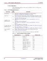
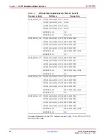
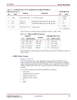
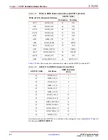
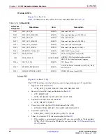
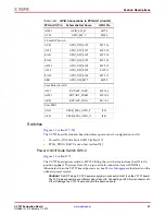
The Ethernet connections from FPGA U1 to the 88E1111 PHY device are listed in
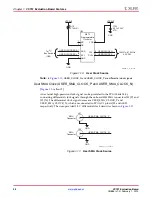
SGMII GTX Transceiver Clock Generation
[
, callout
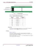
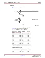
An Integrated Circuit Systems ICS844021I chip (U2) generates a high-quality, low-jitter,
125 MHz LVDS clock from a 25 MHz crystal (X3). This clock is sent to FPGA U1, Bank 113
GTX transceiver (clock pins AH8 (P) and AH7 (N)) driving the SGMII interface. Series AC
coupling capacitors are present to allow the clock input of the FPGA to set the common
mode voltage.
shows the Ethernet SGMII clock source.
Table 1-17:
Board Connections for PHY Configuration Pins
Pin
Connection on Board
Bit[2]
Definition and Value
Bit[1]
Definition and Value
Bit[0]
Definition and Value
CFG0
V
CC
2.5V
PHYADR[2] = 1
PHYADR[1] = 1
PHYADR[0] = 1
CFG1
Ground
ENA_PAUSE = 0
PHYADR[4] = 0
PHYADR[3] = 0
CFG2
V
CC
2.5V
ANEG[3] = 1
ANEG[2] = 1
ANEG[1] = 1
CFG3
V
CC
2.5V
ANEG[0] = 1
ENA_XC = 1
DIS_125 = 1
CFG4
V
CC
2.5V
HWCFG_MD[2] = 1
HWCFG_MD[1] = 1
HWCFG_MD[0] = 1
CFG5
PHY_LED_LINK10
DIS_FC = 1
DIS_SLEEP = 1
HWCFG_MD[3] = 1
CFG6
PHY_LED_RX
SEL_BDT = 0
INT_POL = 1
75/50
Ω
= 0
Table 1-18:
Ethernet Connections, FPGA to PHY Device
FPGA (U1)
Pin
Net Name
M88E1111 PHY U50
Pin
Name
AK33
PHY_MDIO
M1
MDIO
AH31
PHY_MDC
L3
MDC
AL31
PHY_INT
L1
INT_B
AJ33
PHY_RESET
K3
RESET_B
AN2
SGMII_TX_P
A3
SIN_P
AN1
SGMII_TX_N
A4
SIN_N
AM8
SGMII_RX_P
A7
SOUT_P
AM7
SGMII_RX_N
A8
SOUT_N
Содержание VC707
Страница 1: ...VC707 Evaluation Board for the Virtex 7 FPGA User Guide UG885 v1 2 February 1 2013...
Страница 74: ...74 www xilinx com VC707 Evaluation Board UG885 v1 2 February 1 2013 Chapter 1 VC707 Evaluation Board Features...
Страница 94: ...94 www xilinx com VC707 Evaluation Board UG885 v1 2 February 1 2013 Appendix D Board Setup...
Страница 96: ...96 www xilinx com VC707 Evaluation Board UG885 v1 2 February 1 2013 Appendix E Board Specifications...


