


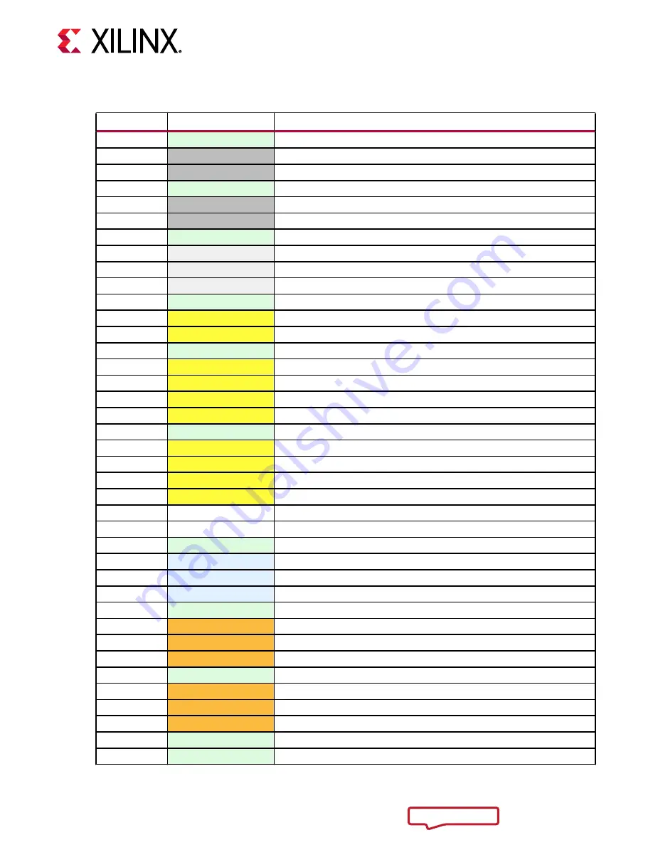
Table 4: SOM240_1 Signal Pins (cont'd)
Pin Number
Signal Name
Signal Description
A8
GND
Ground
A9
HPA12_P
HPIO on bank 66
A10
HPA12_N
HPIO on bank 66
A11
GND
Ground
A12
HPA13_P
HPIO on bank 66
A13
HPA13_N
HPIO on bank 66
A14
GND
Ground
A15
HDA09
HDIO on bank 45
A16
HDA10
HDIO on bank 45
A17
HDA11
HDIO on bank 45
A18
GND
Ground
A19
VCCOEN_PS_M2C
Indication to turn on power for PS I/O peripherals on the carrier card
A20
VCCOEN_PL_M2C
Indication to turn on power for PL /IO peripherals on the carrier card
A21
GND
Ground
A22
JTAG_TMS_C2M
JTAG mode select, pulled up at 1.8V on the SOM
A23
JTAG_TDO_M2C
JTAG data out, pulled up at 1.8V on the SOM
A24
JTAG_TDI_C2M
JTAG data in, pulled up at 1.8V on the SOM
A25
JTAG_TCK_C2M
JTAG clock, pulled up at 1.8V on the SOM
A26
GND
Ground
A27
MODE0_C2M
PS mode bit 0, pulled up at 1.8V on the SOM
A28
MODE1_C2M
PS mode bit 1, pulled up at 1.8V on the SOM
A29
MODE2_C2M
PS mode bit 2, pulled up at 1.8V on the SOM
A30
MODE3_C2M
PS mode bit 3, pulled up at 1.8V on the SOM
A31
Reserved
No connect on the SOM
A32
Reserved
No connect on the SOM
A33
GND
Ground
A34
MIO41
PS MIO signal on bank 501
A35
MIO42
PS MIO signal on bank 501
A36
MIO43
PS MIO signal on bank 501
A37
GND
Ground
A38
MIO61
PS MIO signal on bank 502
A39
MIO62
PS MIO signal on bank 502
A40
MIO63
PS MIO signal on bank 502
A41
GND
Ground
A42
MIO73
PS MIO signal on bank 502
A43
MIO74
PS MIO signal on bank 502
A44
MIO75
PS MIO signal on bank 502
A45
GND
Ground
A46
GND
Ground
Chapter 2: Electrical Design Considerations
UG1091 (v1.0) April 20, 2021
Carrier Card Design for Kria SOM
11