KC724 GTX Transceiver Characterization Board
5
UG932 (v2.2) October 10, 2014
KC724 Board Features
Chapter 1
KC724 Board Features and Operation
This chapter describes the components, features, and operation of the
KC724 Kintex®-7 FPGA GTX Transceiver Characterization Board. The KC724 board
provides the hardware environment for characterizing and evaluating the GTX
transceivers available on the Kintex-7 XC7K325T-3 FFG900E FPGA. The KC724 board
schematic, bill-of-material (BOM), layout files, and reference designs are available online
at:
Kintex-7 FPGA KC724 Characterization Kit website
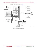
KC724 Board Features
•
Kintex-7 XC7K325T-3 FFG900E FPGA
•
Onboard power supplies for all necessary voltages
•
Terminal blocks for optional use of external power supplies
•
Digilent USB JTAG programming port
•
System ACE™ SD controller
•
Power module supporting Kintex-7 FPGA GTX transceiver power requirements
•
A fixed, 200 MHz 2.5V LVDS oscillator wired to multi-region clock capable (MRCC)
inputs
•
Two pairs of differential MRCC inputs with SMA connectors
•
SuperClock-2 module supporting multiple frequencies
•
Four Samtec BullsEye connector pads for the GTX transceivers and reference clocks
•
Power status LEDs
•
General purpose DIP switches, LEDs, push buttons, and test I/O
•
Two VITA 57.1 FPGA mezzanine card (FMC) high pin count (HPC) connectors
•
USB-to-UART bridge
•
I2C bus
•
PMBus connectivity to onboard digital power supplies
•
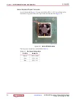
Active cooling for the FPGA


