20
KC724 GTX Transceiver Characterization Board
UG932 (v2.2) October 10, 2014
Chapter 1:
KC724 Board Features and Operation
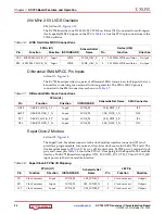
200 MHz 2.5V LVDS Oscillator
,
).
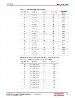
The KC724 board has one 200 MHz 2.5V LVDS oscillator (U35) connected to multi-region
clock capable (MRCC) inputs on the FPGA.
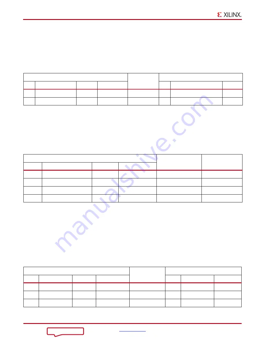
lists the FPGA pin connections to the
LVDS oscillator.
Differential SMA MRCC Pin Inputs
Callout
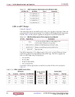
The KC724 board provides two pairs of differential SMA transceiver clock inputs that can
be used for connecting to an external function generator. The FPGA MRCC pins are
connected to the SMA connectors as shown in
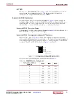
SuperClock-2 Module
Callout
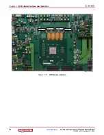
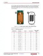
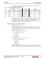
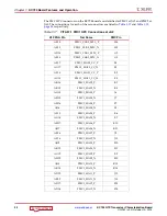
The SuperClock-2 module connects to the clock module interface connector (J82) and
provides a programmable, low-noise and low-jitter clock source for the KC724 board. The
clock module maps to FPGA I/O by way of 24 control pins, 3 LVDS pairs, 1 regional clock
pair, and 1 reset pin.
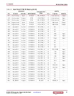
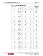
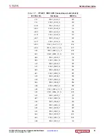
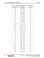
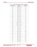
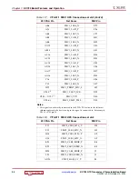
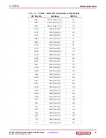
shows the FPGA I/O mapping for the SuperClock-2 module
interface. The KC724 board also supplies UTIL_5V0, UTIL_3V3, UTIL_2V5 and VCCO_HR
input power to the clock module interface.
Table 1-6:
LVDS Oscillator MRCC Connections
FPGA (U1)
Schematic Net
Name
Device (U35)
Pin
Function
Direction IOSTANDARD
Pin
Function
Direction
C25
SYSTEM CLOCK_P
Input
LVDS
LVDS_OSC_P
4
200 MHz LVDS oscillator
Output
B25
SYSTEM CLOCK_N
Input
LVDS
LVDS_OSC_N
5
201 MHz LVDS oscillator
Output
Table 1-7:
Differential SMA Clock Connections
FPGA (U1)
Schematic Net Name
SMA Connector
Pin
Function
Direction
IOSTANDARD
AG29
USER CLOCK_1_P
Input
LVDS_25
CLK_DIFF_1_P
J99
AH29
USER CLOCK_1_N
Input
LVDS_25
CLK_DIFF_1_N
J100
D17
USER CLOCK_2_P
Input
LVDS_25
CLK_DIFF_2_P
J98
D18
USER CLOCK_2_N
Input
LVDS_25
CLK_DIFF_2_N
J101
Table 1-8:
SuperClock-2 FPGA I/O Mapping
FPGA (U1)
Schematic Net
Name
J82 Pin
Pin
Function
Direction
IOSTANDARD
Pin
Function Direction
F11
Clock recovery
Input
LVDS_25
CM_LVDS1_P
1
Clock recovery
Output
E11
Clock recovery
Input
LVDS_25
CM_LVDS1_N
3
Clock recovery
Output
C12
Clock recovery
Input
LVDS_25
CM_LVDS2_P
9
Clock recovery
Output

