KC724 GTX Transceiver Characterization Board
21
UG932 (v2.2) October 10, 2014
Detailed Description
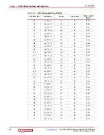
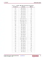
B12
Clock recovery
Input
LVDS_25
CM_LVDS2_N
11
Clock recovery
Output
AJ3
Clock recovery
Output
LVDS
CM_LVDS3_P
17
Clock recovery
Input
AK3
Clock recovery
Output
LVDS
CM_LVDS3_N
19
Clock recovery
Input
D26
Regional clock
Input
LVDS_25
CM_GCLK_P
25
Global clock
Output
C26
Regional clock
Input
LVDS_25
CM_GCLK_N
27
Global clock
Output
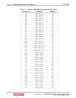
G30
Control I/O
In/Out
LVCMOS18
CM_CTRL_0
61
NC
–
H30
Control I/O
In/Out
LVCMOS18
CM_CTRL_1
63
NC
–
H27
Control I/O
In/Out
LVCMOS18
CM_CTRL_2
65
NC
–
H26
Control I/O
Output
LVCMOS18
CM_CTRL_3
67
DEC
Input
F30
Control I/O
Output
LVCMOS18
CM_CTRL_4
69
INC
Input
G29
Control I/O
Output
LVCMOS18
CM_CTRL_5
71
Align
Input
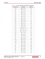
F27
Control I/O
In/Out
LVCMOS18
CM_CTRL_6
73
NC
–
G27
Control I/O
In/Out
LVCMOS18
CM_CTRL_7
75
NC
–
F28
Control I/O
In/Out
LVCMOS18
CM_CTRL_8
77
NC
–
G28
Control I/O
In/Out
LVCMOS18
CM_CTRL_9
79
LOL
H25
Control I/O
Output
LVCMOS18
CM_CTRL_10
81
INT_ALRM
Input
H24
Control I/O
Output
LVCMOS18
CM_CTRL_11
83
C1B
Input
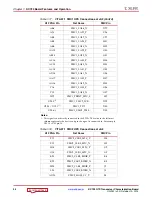
E30
Control I/O
Output
LVCMOS18
CM_CTRL_12
85
C2B
Input
E29
Control I/O
Output
LVCMOS18
CM_CTRL_13
87
C3B
Input
A30
Control I/O
Output
LVCMOS18
CM_CTRL_14
89
C1A
Input
B30
Control I/O
Output
LVCMOS18
CM_CTRL_15
91
C2A
Input
C30
Control I/O
In/Out
LVCMOS18
CM_CTRL_16
93
NC
–
D29
Control I/O
Output
LVCMOS18
CM_CTRL_17
95
CS0_C3A
Input
B29
Control I/O
Output
LVCMOS18
CM_CTRL_18
97
CS1_C4A
Input
C29
Control I/O
In/Out
LVCMOS18
CM_CTRL_19
99
NC
–
A26
Control I/O
In/Out
LVCMOS18
CM_CTRL_20
101
NC
–
A25
Control I/O
In/Out
LVCMOS18
CM_CTRL_21
103
NC
–
A28
Control I/O
In/Out
LVCMOS18
CM_CTRL_22
105
NC
–
B28
Control I/O
In/Out
LVCMOS18
CM_CTRL_23
107
NC
–
B24
CM_RESET
Output
LVCMOS18
CM_RST
66
RESET_B
Input
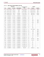
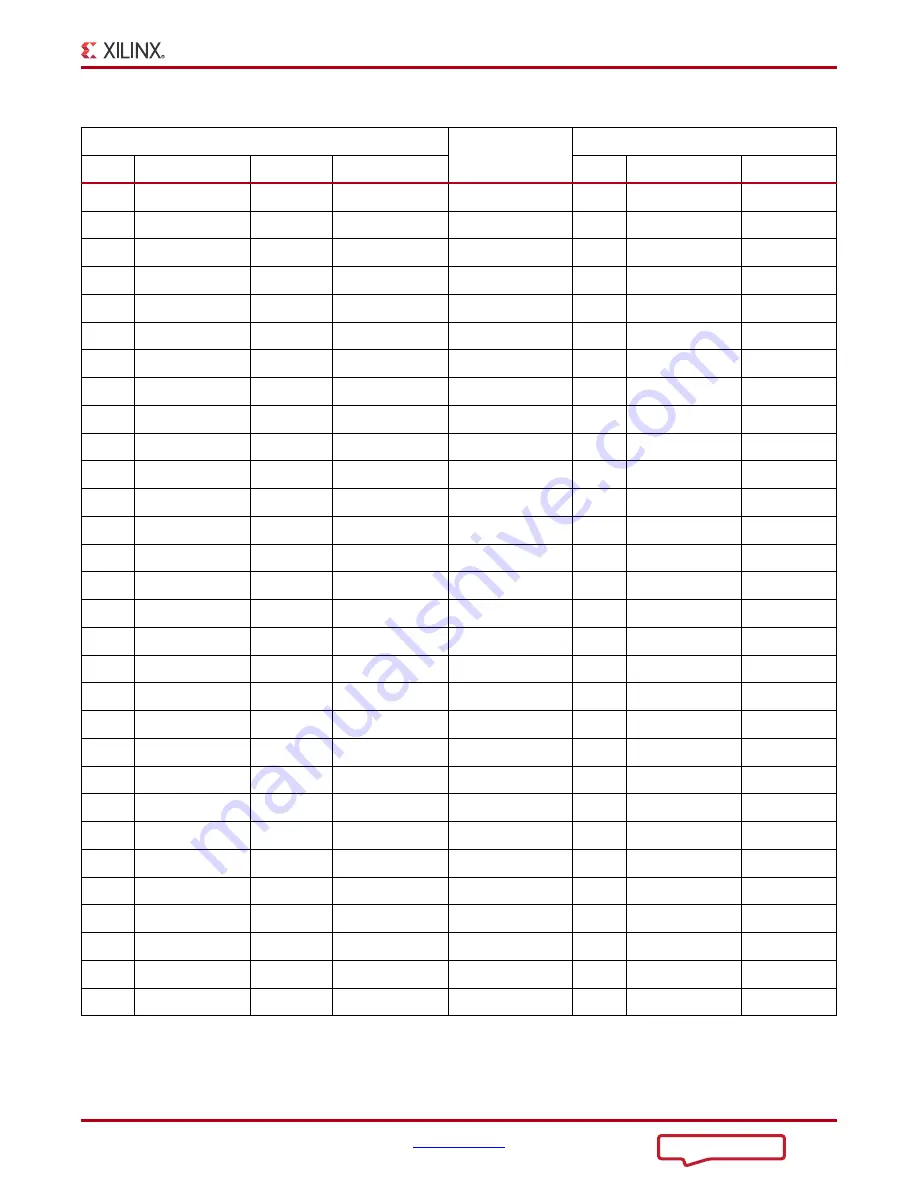
Table 1-8:
SuperClock-2 FPGA I/O Mapping
(Cont’d)
FPGA (U1)
Schematic Net
Name
J82 Pin
Pin
Function
Direction
IOSTANDARD
Pin
Function Direction

