15. Design in guide
15.1. Advice for schematic and layout
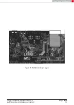
For users with less RF experience it is advisable to closely copy the relating evaluation
board with respect to schematic and layout, as it is a proven design. The layout should
be conducted with particular care, because even small deficiencies could affect the radio
performance and its range or even the conformity.
The following general advice should be taken into consideration:
• A clean, stable power supply is strongly recommended. Interference, especially oscil-
lation can severely restrain range and conformity.
• Variations in voltage level should be avoided.
• LDOs, properly designed in, usually deliver a proper regulated voltage.
• Blocking capacitors and a ferrite bead in the power supply line can be included to filter
and smoothen the supply voltage when necessary.
No fixed values can be recommended, as these depend on the circumstances
of the application (main power source, interferences etc.).
Frequently switching the module on and off, especially with a slowly changing
voltage level of the power supply, can lead to erratic behavior, in rare cases
even as far as damaging the module or the firmware. The use of an external
reset IC can solve this matter and shall be considered especially in battery
operated scenarios.
• Elements for ESD protection should be placed on all pins that are accessible from the
outside and should be placed close to the accessible area. For example, the RF-pin is
accessible when using an external antenna and should be protected.
• ESD protection for the antenna connection must be chosen such as to have a minimum
effect on the RF signal. For example, a protection diode with low capacitance such as
the LXES15AAA1-100 or a 68 nH air-core coil connecting the RF-line to ground give
good results.
• Placeholders for optional antenna matching or additional filtering are recommended.
• The antenna path should be kept as short as possible.
Calypso reference manual version 1.2
© April 2019
www.we-online.com/wireless-connectivity
98


