14
®
ADS7806
ered when choosing the accuracy and drift specifications of
the external resistors. In most applications, 1% metal-film
resistors will be sufficient.
The external resistors shown in Figure 7b may not be
necessary in some applications. These resistors provide
compensation for an internal adjustment of the offset and
gain which allows calibration with a single supply. Not
using the external resistors will result in offset and gain
errors in addition to those listed in the electrical specifica-
tions section. Offset refers to the equivalent voltage of the
digital output when converting with the input grounded. A
positive gain error occurs when the equivalent output volt-
age of the digital output is larger than the analog input. Refer
to Table VIII for nominal ranges of gain and offset errors
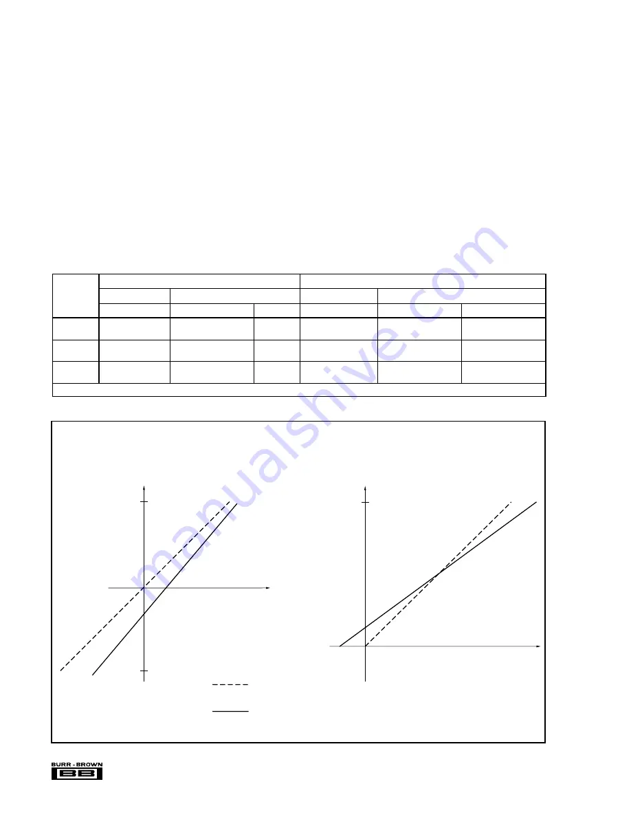
with and without the external resistors. Refer to Figure 8 for
typical shifts in the transfer functions which occur when the
external resistors are removed.
To further analyze the effects of removing any combination
of the external resistors, consider Figure 9. The combination
of the external and the internal resistors form a voltage
divider which reduces the input signal to a 0.3125V to
2.8125V input range at the CDAC. The internal resistors are
laser trimmed to high relative accuracy to meet full specifi-
cations. The actual input impedance of the internal resistor
network looking into pin 1 or pin 3 however, is only accurate
to
±
20% due to process variations. This should be taken into
account when determining the effects of removing the exter-
nal resistors.
REFERENCE
The ADS7806 can operate with its internal 2.5V reference or
an external reference. By applying an external reference to
INPUT
RANGE
W/ RESISTORS
W/OUT RESISTORS
W/ RESISTORS
W/OUT RESISTORS
(V)
RANGE (mV)
RANGE (mV)
TYP (mV)
RANGE (% FS)
RANGE (% FS)
TYP
±
10
–10
≤
BPZ
≤
10
0
≤
BPZ
≤
35
+15
–0.4
≤
G
≤
0.4
–0.3
≤
G
≤
0.5
+0.05
0.15
≤
G
(1)
≤
0.15
–0.1
≤
G
(1)
≤
0.2
+0.05
0 to 5
–3
≤
UPO
≤
3
–12
≤
UPO
≤
–3
–7.5
–0.4
≤
G
≤
0.4
–1.0
≤
G
≤
0.1
–0.2
0.15
≤
G
(1)
≤
0.15
–0.55
≤
G
(1)
≤
–0.05
–0.2
0 to 4
–3
≤
UPO
≤
3
–10.5
≤
UPO
≤
–1.5
–6
–0.4
≤
G
≤
0.4
–1.0
≤
G
≤
0.1
–0.2
–0.15
≤
G
(1)
≤
0.15
–0.55
≤
G
(1)
≤
–0.05
–0.2
Note: (1) High Grade.
OFFSET ERROR
GAIN ERROR
TABLE VIII. Range of Offset and Gain Errors with and without External Resistors
Digital Output
(b) Unipolar
–Full Scale
+Full Scale
Analog Input
Digital Output
(a) Bipolar
–Full Scale
+Full Scale
Analog Input
Typical Transfer Functions
With External Resistors
Typical Transfer Functions
Without External Resistors
FIGURE 8. Typical Transfer Functions With and Without External Resistors.
Содержание PCM-A/D-12
Страница 22: ...4 APPENDIX A PCM A D Parts Placement Guide...
Страница 23: ...5 APPENDIX B PCM A D Parts List...
Страница 26: ...6 APPENDIX C BURR BROWN ADS7806 ADS7807 Datasheet Reprint...
Страница 64: ...7 APPENDIX D PCM A D Demo Software Source Listing...
Страница 73: ...8 APPENDIX E PCM A D Schematic Diagrams...


